
 |
|
Biography
Ambika Prasad Shah was born in Singrauli, Madhya Pradesh, India. He received the B.E. degree in Electronics & Telecommunication Engineering, and M.E. degree in Electronic Engineering from IET, Devi Ahilya University, Indore, India in 2009 and 2015, respectively. He obtained PhD degree from Electrical Engineering Department, IIT Indore, India in 2019. He is currently a post doctoral researcher and his focus is on modeling of reliability issues in semiconductor devices, reliability analysis of digital circuits, and soft error resilient circuit designs.
Utilizing NBTI for Operation Detection of Integrated Circuits
The counterfeiting of integrated circuits (ICs) has increased over the last decades. It affects not only the stable operation of ICs, but can also cause security leaks in electronic systems. This is of particular importance for military, space and financial applications. Unfortunately, it is very difficult to detect recycled ICs, especially when they have been used for only a short period of time.
A new approach could be to take advantage of the aging characteristics of single transistors and the consequences of this on the behavior and power consumption of circuits over time. More specifically, one could make use of the deviation in device performance of single transistors due to Negative Bias Temperature Instability (NBTI) to detect possibly recycled ICs. Due to NBTI, the threshold voltage of a pMOS transistor drifts over time, and thus, if only pure NBTI degradation is considered, the standby leakage current of the transistor decreases concurrently. This decrease in the standby leakage current can be used to detect the total operational time of the IC, as the steady power consumption of the entire circuit also increases slightly.
To demonstrate the proposed methodology, the c17 circuit from the ISCAS’85 benchmark suite has been used to calculate the critical path, which is the path that is exposed to worst-case stress conditions. Steady power consumption under worst-case conditions is compared to steady power consumption in the case of minimum stress. The steady power consumption of the circuit depends mainly on the standby leakage current. Thus, we further analyze the change in the standby leakage current of the c17 benchmark suite with the ongoing operational time by employing the PTM model implemented in HSPICE to estimate the operational time of the chip.
We also calculate the output signal probabilities of all the involved NAND gates based on the input signal probabilities, as shown in Fig. 1. This shows the probabilities of getting logic high at each node of the circuit, P1 through P11. The data flow graph can be used for timing analysis of the c17 benchmark circuit, as shown in Fig. 2. By performing static timing analysis, we note that path I[4]→G2→O[2]→G3→O[3]→G6→O[6] is the critical timing path for the underlying c17 circuit. The longest paths for the c17 circuit are indicated by the enclosed loop line, as also highlighted in Fig. 2. Our results clearly demonstrate that the standby leakage current in worst-case and minimum-stress conditions increases by 20.5% and 10.08%, respectively, after a stress time of three years. Thus, a thorough investigation of the standby leakage current provides a measure with which to analyze the operation of ICs.
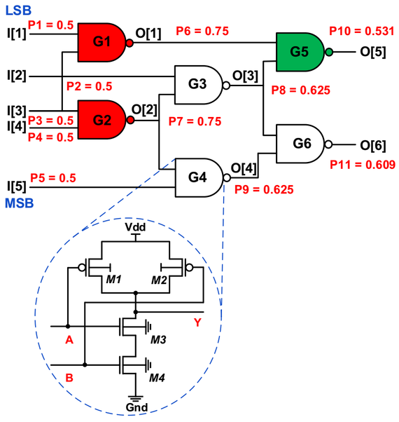
Fig. 1: Input and output signal probabilities for six NAND gates of the c17 circuit. It should be noted that the PMOS devices are stressed when logic 0 is applied at the respective inputs.
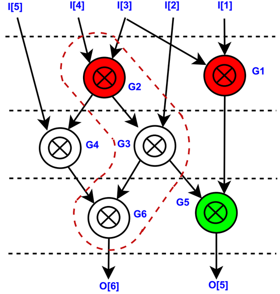
Fig. 2: Data flow graph for the critical path of the c17 benchmark circuit.