 |
|
Biography
Arash Abbasi was born in 1989 in Kermanshah, Iran. He received his Bachelor's degree in Electrical Engineering from the Islamic Azad University in 2011. He received the Master of Science degree in Electronic Engineering from the University Putra Malaysia in 2015, where he worked on radio frequency integrated circuits. After working for four consecutive years in Symmid Corporation as a senior analog designer in the area of IC design he joined the Institute for Microelectronics on February 2019, where he is currently working on his doctoral degree. Arash's main focus is the characterization and modeling of noise in Si technology.
Low-Frequency Noise in Silicon Technology
Low-frequency noise has long been a controversial topic that has attracted the interest of a considerable number of research groups since the beginning of semiconductor technology. Minimizing low-frequency noise in analog applications, such as amplifiers, power management circuits, zero-IF receivers, etc., is crucial for their high performance. So far, their high-performance operation has been guaranteed by either optimizing the design or improving the device technology. In all cases, a detailed understanding of the origin of the noise is mandatory for further optimization.
The most plausible explanation for flicker noise, also known as 1/f noise, is that it is caused by single defects that can become repeatedly charged and discharged, thereby disturbing the current flow path through a single transistor. However, an in-depth understanding of the complex physical mechanism behind charge trapping is of particular importance to estimating its impact on device lifetime and to enhancing transistor fabrication processes. As silicon technology dominates the largest part of the integrated circuit market due to its specific advantages, which are beneficial for low-voltage and low-power applications, there is high demand for Si-based integrated circuits for many analog applications.
The physical mechanisms determining flicker noise are much more complex as compared to the origin of thermal noise, which is well understood. It is commonly accepted that the main source of flicker noise is due to single defects that can dynamically change their charge state and thus give rise to 1/f noise. The defects that are responsible for the observed noise characteristics are either located at the insulator/semiconductor interface or directly in the insulator. As the impact of one single defect on the current through the device can be very small, less than a few microvolts of threshold voltage shift, their characterization is a formidable challenge. While in large-area devices single defects typically cannot be resolved, nanoscale devices enable the monitoring of charge transition events of single defects, as they occur as discrete steps in the drain-source and gate currents. The recorded charge transitions can be analyzed and from them energy barriers and trap levels estimated using our four-state non-radiative multiphonon model. Finally, with the energies and trap levels in hand, one can perform ab-initio calculations that can provide more information about the structure of the defect.
In addition to the study of discrete charge emission events in the drain-source current, the characterization and proper explanation of trap-assisted tunneling (TAT) is also important, especially for low-noise technologies. Although the gate current also slightly increases with the age of the device, it still remains in the deep sub-pico-ampere regime, which is several orders of magnitude smaller than the drain-source currents. Thus, the probing of single charge transitions that contribute to TAT is extremely challenging. In recent reports, the impact of single charges on the gate current was found to be only approximately 2 pA. However, results thus far are still not consistent as it has been found that charge capture transitions visible in the gate current can cause either an increase or decrease in the drain-source current. Accordingly, the investigation of TAT will certainly offer new insights into the physical mechanisms of single defects, which will allow us to further develop our computer models and ultimately to contribute to the improvement of future silicon technologies.
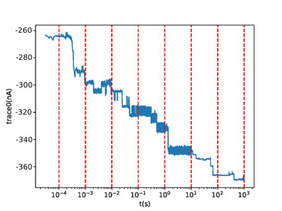
Fig. 1: The stress and recovery sequence of a nanoscale pMOS transistor is shown. As can be seen, the recovery proceeds in a discrete manner. The dotted lines indicate the time points where the sampling rate changes. This non-uniform sampling scheme is required, as usually very long recovery sequences have to be recorded at a high sampling rate per decade. Otherwise, the amount of data produced with a uniform sampling scheme would not be handleable.
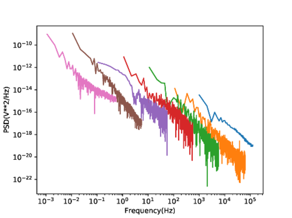
Fig. 2: Noise spectra of the non-uniformly sampled recovery traces. The wider the experimental window gets, the larger the signal-to-noise ratio becomes. It has to be noted that the ultra-low noise floor provided by our custom-made measurement instruments is required to achieve high measurement resolution for single defect characterization.