
 |
|
Biography
Markus Jech was born in Vienna in 1986. He received the degree of Diplomingenieur in Physics from the Technische Universität Wien in 2014. In January 2015 he joined the Institute for Microelectronics, where he is currently working on his doctoral degree.
New Insights into the Physics of Hot-Carrier Degradation in MOSFETs
A major reliability issue in modern CMOS technology is hot-carrier degradation (HCD). It is widely accepted that hot-carrier damage is due to the breaking of Si-H bonds at the Si-SiO2 interface, resulting in electrically active traps. Although this detrimental phenomenon has been known for decades, there is still no consensus on the underlying physics of the defect creation mechanism. Almost two decades ago, a series of papers by the group of Hess marked a breakthrough in the modeling of HCD in electronic devices. The key idea and assumption of the model is to link a thorough carrier transport treatment with two different but interacting regimes for defect creation.
According to Hess, Si-H bond breakage is driven by a single particle (SP) and a multiple particle mechanism (MP). The SP process accounts for the high energy fraction of the carrier ensemble, where a single carrier triggers the desorption of hydrogen. On the other hand, the MP mechanism describes a subsequent ladder climbing process, induced by several carriers with moderate energies. However, no details about the underlying physical principles are given. These ideas have been picked up by other groups and have served as the basis for further model developments.
Interestingly, since then, the understanding of how electrons interact with the Si-H bonds has not developed further, although Hess speculated that a resonance-based process could be the main reason for HCD. To reveal the actual physics behind HCD, we reviewed the wealth of information available on the interaction of electrons and adsorbates on an Si-surface. STM studies, with their tuneable carrier energies, clearly suggest that there is an unambigious connection between experimentally observed Si-H bond breaking processes and HCD in electronic devices. Indeed, a resonance scattering process, whereby an electron localizes in the vicinity of the Si-H bond and excites its phonon modes, together with a vibrational heating mechanism (see Fig. 1), seems to be the main cause for hot-carrier induced damage. The moderate carrier energies needed for this excitation channel, together with its strong current dependence, agree well with the characteristic features of hot-carrier effects in MOSFETs.
Such a description considers neighboring transitions (ladder climbing), as well as transitions to higher excited states (over-tone transitions), and is therefore fully consistent with the previously mentioned SP and MP mechanism. Additionally, it allows for an intuitive understanding of another peculiarity of HCD. Occasional reports show that the degradation caused by HCD for nMOS devices is larger than for pMOSFETs. If the accessible resonance state for holes is higher in energy than that of electrons – as suggested by different atomistic studies – it is less likely for holes to trigger bond excitation and dissociation (see Fig. 1).
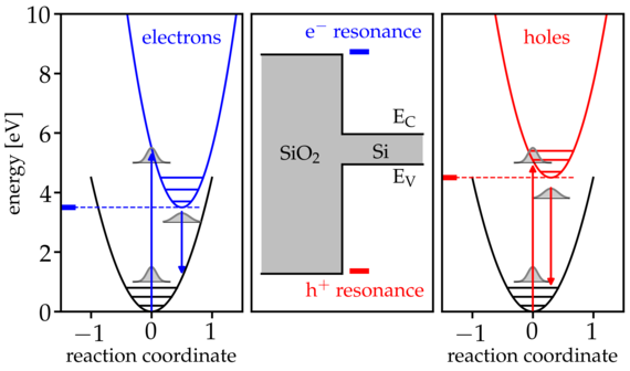
Fig. 1: Schematic representation of the resonance scattering process. A carrier is able to localize in the vicinity of the Si-H bond, via an accessible resonance state, which changes the Si-H potential to an excited state. Upon relaxation, the bond is left in a vibrationally excited state. If the accessible electron resonance (left) is lower in energy than the hole resonance (right), electrons in nMOS devices cause potentially more damage.