 |
|
Biography
Xaver Klemenschits was born in Vienna in 1994. He studied Nanoscale Physics at the University of Birmingham, England, for which he received the degree of MSci in 2017. He joined the Institute for Microelectronics in August 2017, where he is working on topography simulation using different deposition and etching models.
Advanced-Node Dielectric Metal Gate Process Simulation using ViennaTS
Semiconductor device dimensions have been decreasing steadily over the past several decades, generating the need to overcome fundamental limitations both to the materials they are made of and the fabrication techniques used to build them. Modern metal gates are no longer a simple polysilicon layer, but rather consist of a stack of several different materials, each often requiring multiple processing steps to obtain the characteristics required for stable operation. In order to better understand the underlying mechanics and predict the potential of new methods and materials, technology computer-aided design has become increasingly important.
The semiconductor process simulator developed at the Institute for Microelectronics, ViennaTS, is used to create chemical models that can simulate the reactions taking place in the reactor and on the wafer surface. These govern how materials are modified during process steps, such as the etch or deposition rates at each point of the wafer, to generate the final surface profile. By carefully tuning these chemical models, even complex fabrication steps can be simulated accurately, which is becoming increasingly important with the use of more advanced processing steps. One approach to creating nanometer transistors with better electrical characteristics is the stacking of multiple channels, switched by a single gate surrounding them. Generating such a structure from a flat wafer requires more than 30 processing steps, which include highly complex chemical reactions and the influence of residues left by an earlier process on the next. The structure generated by these process steps, simulated with ViennaTS, can be seen in Figs. 1 and 2. The structures generated by ViennaTS can then be passed to a device simulator to evaluate electrical characteristics and fine-tune the fabrication process.
Recently, ViennaTS was ported to the web using a current standard for portable high-performance applications: WebAssembly. This standard allows C/C++ codebases to be compiled for execution in browser engines and thus enables client-side execution of the application. This version of ViennaTS, which can be tested directly in-browser, is available here.
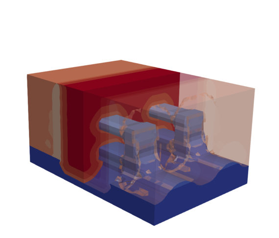
Fig. 1: Stacked nanosheet gate-all-around transistor geometry generated by ViennaTS.
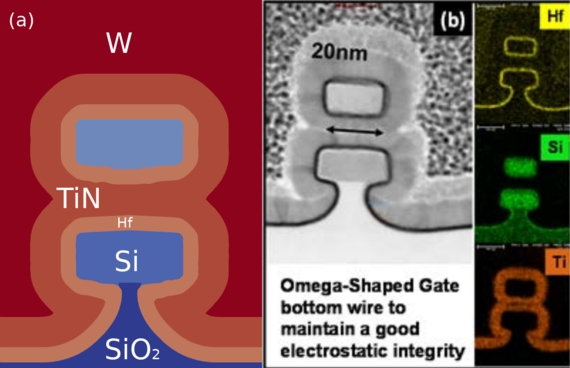
Fig. 2: Comparison of a) an experimentally generated structure and b) the simulated structure by comparing the slice perpendicular to the silicon channels. [b) taken from here.]