 |
|
Biography
Theresia Knobloch was born in Vienna in 1992. She received her BSc degree in Technical Physics and the degree of Diplomingenieur in Microelectronics from the Technische Universität Wien in 2014 and 2016, respectively. She joined the Institute for Microelectronics in April 2016, where she is currently working on her doctoral degree. Her current research topic are novel devices based on two-dimensional materials.
Hysteresis in MoS2 MOSFETs
Hysteresis in the transfer characteristics of metal oxide semiconductor field-effect transistors is a well-known phenomenon. In the context of field-effect transistors, hysteresis in the transfer characteristics refers to a shift in the threshold voltage of the device depending on the device's history. Typically, the threshold voltage of the up-sweep is different from the threshold voltage of the down-sweep, thus the threshold voltage depends on whether the device was in the on or off state before switching. This situation is shown in the characteristics displayed on the left side of Fig. 1, where the threshold voltage for the up-sweep amounts to -4V and for the down-sweep to 5V. When using field-effect transistors as voltage-controlled switches in conventional digital logic circuitry, the threshold voltage is a central design parameter. This implies that any change in the threshold voltage is detrimental and might cause circuit failure. This explains why hysteresis in the transfer characteristics has long been considered an undesirable effect and has to be reduced to an absolute minimum before any transistor technology is mature enough for digital logic applications. However, controllable hysteresis could be a key element in new device concepts for neuromorphic circuit applications. Neuromorphic computing abandons the strict separation between computational and memory units, making transistors that simultaneously provide a memory-like feature in the form of hysteresis a possible basis component. For this purpose, the hysteresis must be very stable and switch repeatedly to one voltage for the up-sweep and to another voltage for the down-sweep.
An enhanced understanding of the physics behind this phenomenon is urgently required in order either to reduce hysteresis to a minimum level or to engineer a fixed hysteresis width spanned by two constant threshold voltages. To increase the physical understanding of hysteresis, we systematically measured it in top-gated molybdenum disulfide (MoS2) MOSFETs and modeled the characteristics using a drift-diffusion based TCAD approach. In Fig. 1, the measurement points are compared to the simulations depicted as lines. On the right side, the hysteresis width's strong dependence on the sweep range is shown. The hysteresis width is defined as the difference between the threshold voltages for the up- and for the down-sweep. Hysteresis strongly increases when the sweep range is extended to higher gate voltages. In Fig. 2, the hysteresis width is shown as a function of the measurement frequency. The measurement frequency is the inverse of the total time for one complete measurement sweep. Higher frequencies and smaller sweep ranges correspond to smaller hysteresis widths, albeit the dependence on the frequency is less pronounced than the dependence on the sweep range. This fact can be easily explained when attributing hysteresis to charge transfer reactions of charge carriers to defects in the amorphous aluminum dioxide serving as a gate dielectric. We use a non-radiative multi-phonon model to describe charge capture and emission events at oxide defects, and the good agreement between measurement and simulation demonstrates that the model can explain both – the strong bias dependence, as well as the sweep frequency dependence.
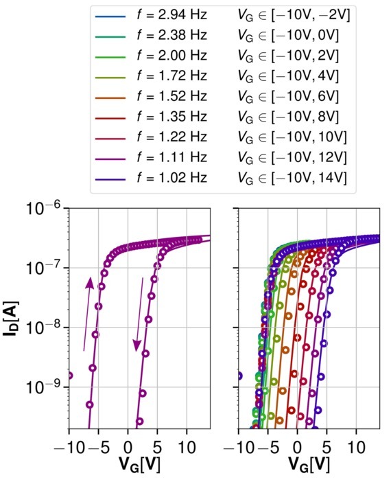
Fig. 1: The transfer characteristics of MoS2 MOSFETs obtained from measurement (circles) and simulation (solid lines). For both the measurements and the simulations, a full sweep always started at negative voltages, moved to positive voltages and then back to negative voltages. The right side shows the characteristics for different maximum top gate voltages.
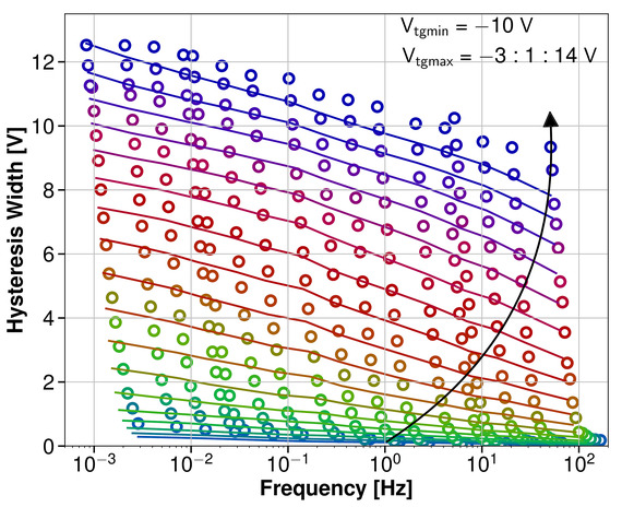
Fig. 2: The hysteresis width's dependence on the sweep frequency. The symbols and lines correspond to measured and simulated hysteresis widths, respectively. The color coding used for different sweep ranges in this figure corresponds to the colors used in Fig. 1, thus the sweep range decreases from dark blue through red and green towards light blue, which represents the smallest sweep range.