 |
|
Biography
Jakob Michl was born in Freistadt, Austria, in 1993. He received his MSc degree in Physics from the University of Vienna in 2018. He joined the Institute for Microelectronics in January 2019, where he is currently working on his doctoral degree.
Operation of Silicon Transistors at Cryogenic Temperatures
Metal-oxide-semiconductor (MOS) devices are used in all integrated electronic circuits, and their characteristics and performance have therefore been extensively studied for several decades. While commercial electronic devices are designed to work at room temperature, or at least within a narrow temperature range (typically -25 C to 125 C), new technologies, which are developed for quantum computing control systems or specialized instruments for astronomy, are expected to operate stably also at cryogenic temperatures. For this new temperature regime, where temperatures down to only a few Kelvin are needed, outstanding characteristics in terms of on-state current, leakage current, subthreshold swing or transconductance have been reported for many structurally different devices (MOSFETs, FinFETs, SiGe FETs, etc.). Nevertheless, to improve existing technologies further, an understanding of the physical mechanisms determining device behavior is inevitable. This also implies the development of physics-based models for detailed computer simulations of single MOS transistors intended for operation at such cryogenic temperatures.
It seems likely that a significant contributor to the deviations from ideal device characteristics observed at cryogenic temperatures is due to single defects in the amorphous insulator and its interface with the semiconductor. We therefore examine the defect ensemble prevalent in large-area MOSFETs to better understand the general trends in the electrical properties, i.e. drift of the threshold voltage. Quite interestingly, the first measurement results have revealed a saturation of the subthreshold swing, which has been recently proposed to exist theoretically in several low-temperature studies. This limit, which is about a factor of 10 higher than the Boltzmann theoretical thermal limit, could originate from a low interface trap density at cryogenic temperatures. This would explain the offset of the subthreshold swing and confirms the crucial role of single defects in devices especially at cryogenic temperatures.
For a systematic investigation of bulk and interface traps, Bias Temperature Instability (BTI) measurements play a central role. Continuous threshold voltage shifts, which are typically observed when BTI is studied on large-area devices, are used to estimate the impact of defects on device behavior. Time-dependent defect spectroscopy allows for the characterization of single defects in nanoscale structures and can provide additional information on the defects and aid in the development of a detailed physical understanding of relevant processes. It is generally likely that well-established temperature dependencies around room temperature behave differently at low temperatures. Understanding these dependencies is necessary in order to find the optimal trade-offs in the design of future technologies.
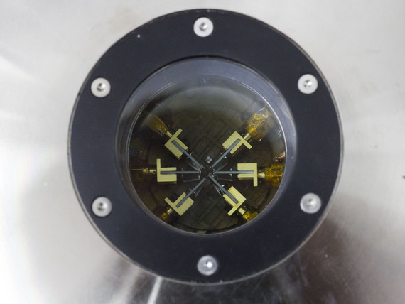
Fig. 1: Cavity of a cryogenic probe station that allows measurements at temperatures down to 3.7 K (Copyright: TU Wien).
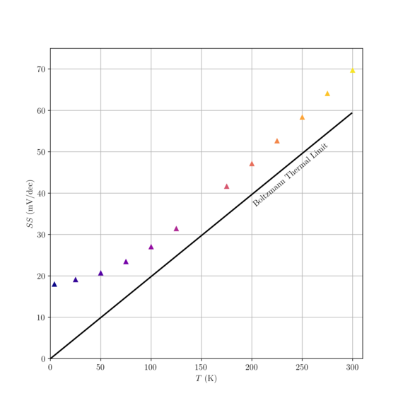
Fig. 2: Subthreshold swing (SS) of an Si nMOS transistor within the temperature range of 4 K to 300 K. At low temperatures, the SS tends to saturate and no longer follows the Boltzmann thermal limit.