
 |
|
Biography
Amirhossein Moshrefi was born in Iran in 1990. He studied Electrical Engineering at Amirkabir University of Technology, Iran, where he received the Master's of Science degree in 2014. Afterwards, he joined the Nano-electronics Center of Excellence at the University of Tehran, Iran, in September 2015, where he enrolled the PhD program in electrical engineering. Currently he is visiting the Institute for Microelectronics at TU Wien. His research focuses on compact modeling of bias temperature instabilities for integrated electronic devices.
Consideration of the Impact of Single Defects in Circuit Simulations
As the scaling of transistor geometries towards only a few tens of nanometers continues, we find that small devices face new challenges in regards to their reliable operation. Compared to large-area transistors, where device-to-device variations of the drift in the threshold voltage do not play a crucial role for circuit simulations, the large variations in terms of the drift in the threshold voltage observed for nanoscale technology nodes might be of particular importance for the high performance operation of integrated circuits. These variations arise from the fact that in scaled nodes the impact of single defects is significantly enhanced, such that single charge transition events can be observed as discrete changes in the device behavior. The models that are widely implemented in circuit simulators rely on describing the average behavior of a certain technology but do not explicitly consider the impact of single point defects on the behavior of individual devices. To study these defects, random telegraph noise (RTN) measurements - an equilibrium characterization technique - or stress-recovery experiments that enable the characterization of the commonly studied bias temperature instabilities (BTI) are typically performed. For the proper explanation of the features associated with degradation mechanisms, several physical models have been developed. For instance, to explain RTN signals, as shown in Fig. 1, Markov chains with two to four states have been found to be suitable. While the modeling of a simple RTN signal is possible with a two-state Markov process, single defect investigations also revealed so-called temporary RTN behavior, which requires an additional metastable state for its proper explanation. Intricate features of single defects such as these are typically not considered by state-of-the-art circuit simulators but are assumed to be an essential ingredient when considering nanoscale technologies.
In integrated circuits, both phenomena, namely RTN and BTI, play an important role. In particular, one has to consider negative BTI, which mainly affects pMOS transistors, and positive BTI, which mainly affects nMOS transistors, in integrated CMOS circuits. Although experimental studies on BTI have revealed that NBTI for pMOS transistors is much more pronounced as compared to the PBTI/nMOS case, both effects have to be considered for a consistent description of BTI. However, considering the impact of BTI on the behavior of complex circuits at the single defect level is a formidable challenge. For instance, as the defects exhibit charge transition times that strongly depend on the applied bias, a purely digital simulation would lead to inaccurate results. For precise AC simulations, the time resolution of the applied signal is a crucial parameter. A high time resolution may lead to large simulation times for long AC signals. Furthermore, an insufficiently finely resolved time axis may lead to an underestimation of the drifts of the threshold voltage. Also, as each device contains several single defects, the transition probability for each defect has to be computed at each time step, which can easily become computationally very expensive for large circuits. In addition, the charge feedback of single defects on other defects in their vicinity has recently been found to be important and requires a self-consistent simulation at the single transistor level.
To describe the device physics at the circuit level in a manner that is compatible with state-of-the-art circuit simulators, a Verilog-A module has to be implemented. This module will describe the charge transfer reactions of single defects using non-radiative multi-phonon theory, enabling one to describe RTN and BTI. For this, the model has to be calibrated against experimental data to determine the distribution of trap levels and energy barriers. The applied biases are provided by the SPICE simulator. Finally, parameters, like circuit performance, power consumption and jitter, can be studied in detail for arbitrary input signals, considering single defects for the first time at this level.
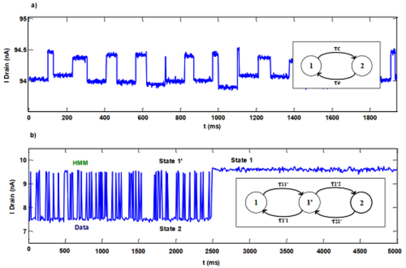
Fig. 1: a) An ordinary RTN signal can be described by a two-state Markov process. b) However, RTN signals that exhibit certain periods of inactivity have been found. The description of these signals requires an additional state and can thus be properly explained by a three-state Markov process.
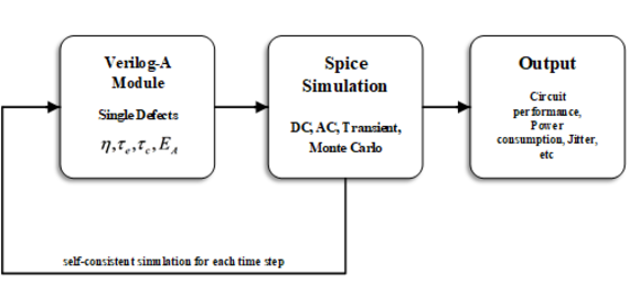
Fig. 2: The simulation tool chain targeted by our circuit simulation approach. The Verilog-A module describes the behavior of the individual devices and is called by the SPICE simulator. This allows one to analyze the performance of the circuit for arbitrary input signals and to consider the impact of single defects on the device behavior.