 |
|
Biography
Bernhard Stampfer, born in 1989 in Austria, studied at the Technische Universität Wien where he received the BSc degree in Electrical Engineering (2013) and the Diplomingenieur degree in Microelectronics and Photonics (2016). He joined the Institute for Microelectronics in March 2016, where he is working on his doctoral degree.
Defect Spectroscopy using Capacitance-Voltage Measurements
The reliability of modern MOS transistors is strongly affected by single defects located in the oxide or at the interface between the insulator and the semiconductor bulk material. These defects are unavoidably introduced during device manufacturing and are often a consequence of the amorphous nature of the oxide. During the operation of the device, these single defects are able to change their charge state by exchanging a charge with the channel or the gate contact. These charge transitions change important operational parameters of the device, such as the threshold voltage or subthreshold slope, and to some extent may cause the whole complex circuit in which the devices operate to fail. Physically accurate models explaining the behavior of these defects are necessary to minimize the influence of defects during the design stage, to properly predict the lifetime of devices and to define safe operating conditions.
The capacitance-voltage (CV) characterization method used here allows one to characterize these defects and aids in the development of highly accurate defect models. Compared to other characterization methods, such as time-dependent defect spectroscopy or random telegraph noise analysis, the advantage of the CV method is that it not only allows one to study the net effect of the degradation, but also enables one to investigate the evolution of the density of defect states in energy. This is a considerable advantage for developing new and verifying existing defect models.
The CV method aims to record CV curves (small signal capacitance over gate bias) of a device between periods of operation, i.e. stress, at elevated temperatures and biases, as shown in Fig. 1 (top). The defects in the device that are close to the Fermi level when bias is applied will increase the observed capacitance as they respond to the AC signal. By mapping the applied gate bias to the surface potential, i.e. to the Fermi level at the interface, as shown in Fig. 1 (middle), and comparing the difference in capacitance with a reference curve recorded at the beginning of the measurement series, the evolution of the trap density can be extracted, see Fig. 1 (bottom). Challenges for this characterization method include performing accurate and repeatable CV measurements and finding a reliable method of mapping the gate bias to the surface potential.
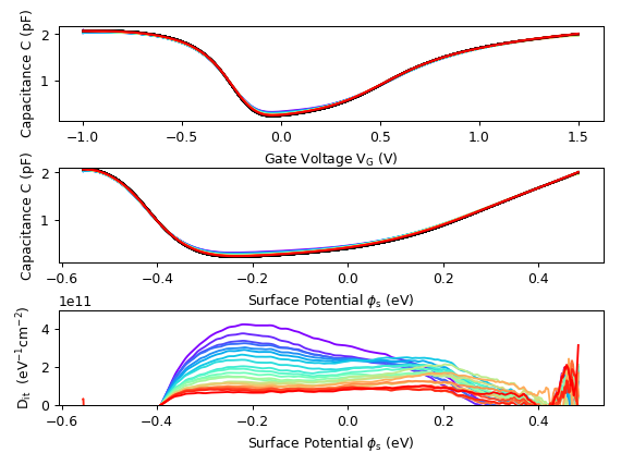
Fig. 1: Top: Evolution of the gate capacitance of an Si-SiO2 pMOS transistor operated at elevated temperatures and gate biases. Middle: Same again, but the gate is bias mapped to the surface potential of the transistor. Bottom: Extracted change in density of equivalent interface states during the measurement.