 |
|
Biography
Alexander Toifl was born in St. Pölten, Austria, in 1993. He studied at the TU Wien where he received the BSc. degree in Electrical Engineering (2016) and the Diplomingenieur degree in Microelectronics and Photonics (2018). He joined the Institute for Microelectronics in August 2018 as a research assistant. Alex's scientific interests include computational modeling (post-implantation annealing of GaN and SiC) and high performance numerical approaches (non-planar epitaxy) for process TCAD.
Level-Set Based Anisotropic Etching Simulations
Anisotropic etching of silicon (Si) with wet etchants (e.g. potassium hydroxide (KOH) and tetramethylammonium hydroxide (TMAH)) is an important semiconductor processing technique that utilizes the crystalline nature of the material. While KOH etching is known mainly for its application in the production of micro-electromechanical systems, the technique plays an important role for embedded silicon germanium (e-SiGe) in source/drain (S/D) engineered sub-28 nm node metal-oxide-semiconductor field-effect transistors (MOSFETs). By employing a combination of dry and wet etching, an S/D cavity formed by the characteristic {111}-planes can be produced. The exact geometry of the resulting sigma-shaped cavity determines the uniaxial strain in the MOSFET channel after epitaxial growth of SiGe. Thus, it is very important to control the critical design variables (i.e. tip depth, channel-cavity distance and cavity depth).
In order to optimize the fabrication steps for sigma-shaped cavities, process technology computer-aided design (TCAD) is very valuable. We employ the level-set method, where the wafer surface is described by the zero level-set of the function and the time evolution is determined by the level-set equation. The level-set equation assumes the form of a Hamiltonian-Jacobi equation, which critically depends on a speed function defined by the highly anisotropic etch rates. The speed function is constructed using a linear interpolation, which defines a spatially strongly varying function and thus leads to a numerically demanding non-convex Hamiltonian. In order to enable stable and physically relevant numerical solutions, we employ a novel dissipative local Lax-Friedrichs scheme, which is based on information about the local geometry and the nature of the speed function (Fig. 1).
The dissipation scheme allows us to simulate the sigma-cavity by Qin et al. (Microelectron. Eng., vol. 181, pp. 22–28, 2017), which employs a two-step reactive ion etching step and a sequential wet etching step (Fig. 2). The characteristically small etch rate of {111} planes gives rise to a final profile consisting of two {111} planes that define a sharp corner at a certain position relative to the channel (sigma-cavity tip). The associated design parameters, tip depth and channel-cavity distance (Fig 3.), are accurately predicted by the dissipation scheme. Furthermore, we compare our scheme with an elemental approach, which only takes the local speed function and level-set normal into account. The elementary approach results in insufficient dissipation beneath the spacer and gate stack, which results in an artificially high undercut rate. In contrast, the proposed scheme reproduces the physical undercut and thus is able to correctly predict the geometry of the sigma-shaped cavity.
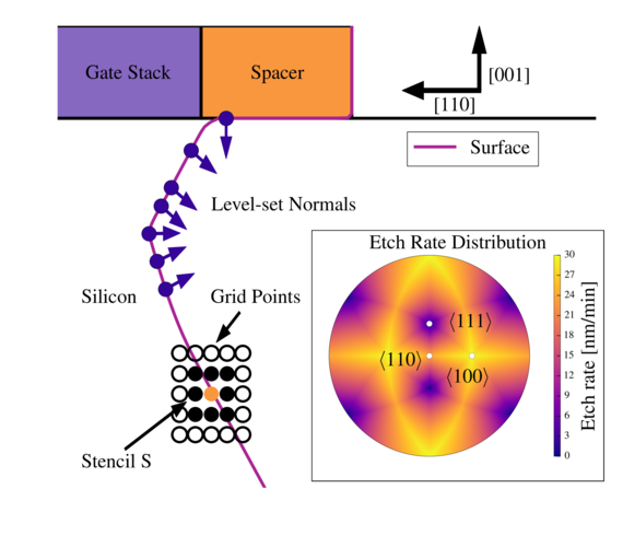
Fig. 1: The proposed dissipation scheme is based on normals and the associated speed functions, which are calculated for a stencil consisting of the central grid point and its immediate neighbors. The inset visualizes the highly anisotropic etch rate distribution associated with TMAH.
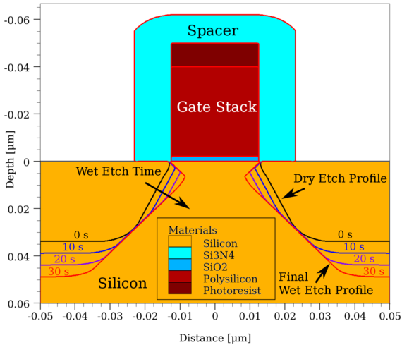
Fig. 2: The temporal evolution of the etch profile. During the self-limiting wet etch, the slow-moving {111} planes form the sigma-shaped cavity.
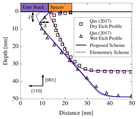
Fig. 3: The etch profiles presented by Qin et al. are accurately reproduced using the proposed scheme. In contrast, the elementary scheme starting from the same dry etch profile results in artificially high undercut.