 |
|
Biography
Michael Waltl was born in Oberndorf near Salzburg, Austria. He received the BSc degree in electrical engineering, the degree of Diplomingenieur in microelectronics, and the doctoral degree in technical sciences from TU Wien in 2009, 2011, and 2016, respectively. His scientific focus is on experimental characterization and modeling of reliability issues prevalent in semiconductor devices and devices with more exotic 2D materials. In this field, he primarily studies bias temperature instabilities in modern transistors. He also leads the device characterization laboratory at the institute, where he is in charge of developing electrical measurement methods.
Single-Defect Spectroscopy in Wide-Bandgap Transistors
In semiconductor transistors, Bias Temperature Instabilities and hot-carrier degradation are amongst the most extensively studied phenomena seriously affecting device time-to-failure. Both effects occur at nominal operating conditions and degrade the performance of each individual transistor. To study these phenomena, changes in the IDVG characteristics or drifts in the threshold voltage are typically monitored and analyzed. Before the sequences are measured, defined stress sequences are applied, in order to deliberately cause device performance degradation.
By using stress-recovery sequences, drifts in the threshold voltage have been widely studied employing large-area and nanoscale transistors. While large structures exhibit a continuous drift in the threshold voltage, the recovery of nanoscale devices proceeds in a discrete manner. Each of the discrete steps visible in the recovery traces can be attributed to a change in the charge state of a single defect. These single defects have already been investigated in considerable detail for silicon transistors, taking advantage of the availability of structures several tens of nanometers small. As the impact of a single charge transition significantly decreases with increasing gate area, however, resolving those steps in larger structures is very challenging.
A promising way in which to investigate single defects in large structures has been demonstrated in the case of gallium nitride (GaN) fin-metal insulator semiconductor (MIS) high-electron-mobility transistors (HEMTs), where measurements have been performed at cryogenic temperatures. The low temperatures are especially beneficial for defect characterization as the charge transition times of a very large number of defects exceed our measurement window at room temperature and thus do not show up in our experimental data, and a smaller number of defects are active, which enables single defect analysis in defect rich structures. By analyzing the provided GaN HEMTs, we could clearly observe random telegraph noise signals of single defects (see Fig. 1).
Upon closer inspection, it can be seen that the defect pairs A/B and C/D show similar step heights and that defect A(C) triggers defect B(D). In addition, the similar step heights and the correlated behavior indicate that these traps are located in the vicinity of each other, which gives rise to an intricate electrostatic coupling of the single defects. The strong coupling between the defects is also reflected in the similar temperature dependence and bias dependence of their charge transition times. From the measurement data, their trap positions can be estimated by considering the slopes of the bias dependence of their charge capture time characteristics, as shown in Fig. 2. As the slope is very weak for all four defects, they are estimated to reside in the AlGaN barrier close to the channel.
Overall, a detailed study of single defects reveals a multitude of interesting mechanisms that could not otherwise have been observed by studying large-area devices. In addition to the previously observed volatile behavior of defects, electrostatically coupled defects could be found in GaN MIS HEMTs. To describe the coupling, self-consistent simulations have to be performed.
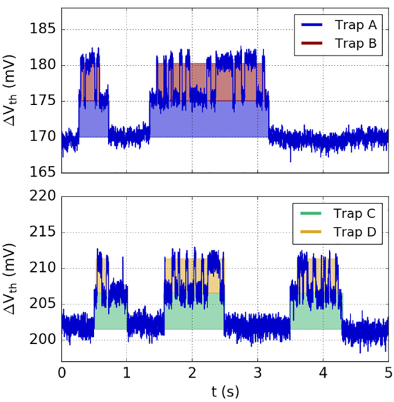
Fig. 1: The threshold voltage shifts can be calculated from the recorded drain-source current by using the initial IDVG characteristics. Quite interestingly, the slower defects, B and D, are only active if defects A and C have captured an electron.
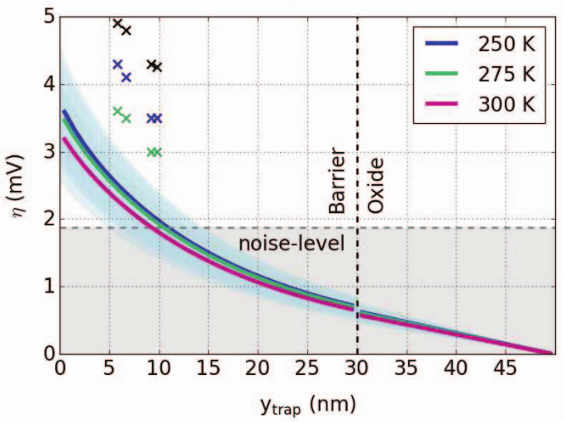
Fig. 2: To estimate the trap positions, TCAD simulations, wherein a single defect is placed along a horizontal cut below the hetero junction interface, are performed. These simulations suggest that the analyzed single defects are located close to the channel/barrier interface. The variation in the trap levels can be calculated from random discrete dopant simulations (shaded area).