4.6 Calibration
Whether or not DG reproduces confinement correctly largely depends on the boundary conditions, the
mesh spacing and the parameters λn for electrons and λp for holes. As stated in the last section, Robin
boundary conditions at insulator-semiconductor interfaces have proven to be best suited since they
deliver the best fit with the carrier concentrations obtained from a solution of the Schrödinger
equation (cf. Section 2.6).
4.6.1 Calibration for the Drift Diffusion Model
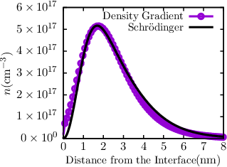
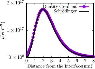
In Figure 4.1 the results of a fit, with a density gradient quantum corrected drift diffusion model, for
electrons are shown for various grid spacings. This figure clarifies the need for a finely spaced grid for
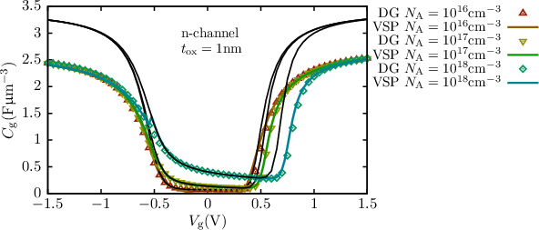
simulation, when using a quantum correction model. In Figure 4.4 Capacitance-Voltage curves,
obtained by density gradient and a Schrödinger-Poisson solver, for n- and p-channel 1D MOS
structures for various dopings are shown and compared [90]. Since density gradient does not exhibit a
free, doping dependent parameter, a set of parameters only works for a certain bulk doping [5]. This
is the main disadvantage of density gradient. Another requirement of density gradient, as for any
Schrödinger-Poisson solver, is that the grid needs to be in the sub-nanometer regime in
order to fully refine the 2D electron gas in a MOS structure, as demonstrated in Figure
4.1.
4.6.2 Calibration for a SHE of the BTE
This section is devoted to the calibration of density gradient in ViennaSHE [65]. To this end
Robin-Boundary conditions and the simple scheme have been implemented and a comparison with
VSP [51] has been carried out in weak inversion. The parameters of the fit are given in Table 4.1 and
the resulting calibration is shown in Figure 4.3.
| Carrier Type | α | β | f |
|
|
|
|
| Electrons | -61.3V∕m | -11.4⋅10-5V | 0.0 |
| Holes | -36.9V∕m | -8.3⋅10-5V | 0.0 |
| Table 4.1: | Robin boundary condition parameters for density gradient and SHE. The
parameters have been obtained by manual optimization using VSP [51]. |