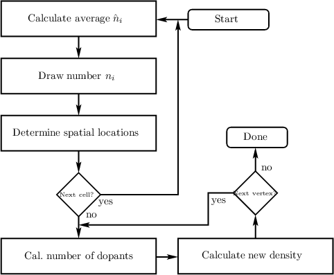
| Figure 5.1: | A flowchart of the Monte Carlo algorithm for random discrete dopants detailed in the text. |
As stated above, in sub-100nm field effect devices, the discreteness of the dopant atoms cannot be ignored anymore. In modern semiconductor devices, the semiconductor doping is introduced by ‘ion implatation’. In this technique the semiconductor material is bombarded by ionized dopant atoms. Upon hitting the target material the dopant atoms are randomly scattered by the lattice atoms of the semiconductor. Thus, to obtain the positions of the dopant atoms, in an ion-shell model of the atom, one can either directly use the data from a process simulation or discretize the given macroscopic doping density (NA and ND) and calculate the dopant positions by a straight-forward Monte Carlo algorithm [96, 95].
In this thesis the Monte Carlo approach to the placement of random discrete dopants is chosen. The algorithm works as follows (cf. Figure 5.1).
| Figure 5.1: | A flowchart of the Monte Carlo algorithm for random discrete dopants detailed in the text. |
First the expected number of dopants  i is calculated per cell i using
  i = V i ×Ni, where Ni is the
dopant concentration and V i is the volume of the cell. Next, the actual number of dopants of the ith
cell is obtained by drawing a Poisson distributed (
i = V i ×Ni, where Ni is the
dopant concentration and V i is the volume of the cell. Next, the actual number of dopants of the ith
cell is obtained by drawing a Poisson distributed ( i being the mean value) random number ni, which
is the total number of dopants in that cell. In a third step the positions of each of the ni dopants are
determined by drawing random numbers for each spatial direction under the condition that each
position must be located within the boundaries of the cell. Since in Poisson’s equation charge densities
are needed, equivalent charge densities have to be calculated from the positions of the
dopants. When using a finite volume discretization for Poisson’s equation this is done by
finding the vertex with the shortest distance to each dopant and counting the number of
dopants (j) associated with each vertex (cf. Figure 5.2). Then, after the dual grid has
been calculated, the new donor/acceptor concentrations per volume in the dual grid is
calculated by dividing the number of dopants j associated with the vertex at the center of
the finite volume by the volume. The precision of this algorithm strongly depends on the
resolution of the grid. In [93] it has been shown that a grid with a spacing below 1nm is
sufficient to capture the mean value of the threshold voltage variability due to RDD in
field effect devices. This results in a ‘jittered’, finely resolved doping, which is suitable for
simulation of RDD with conventional device simulators employing Poisson’s equation.
i being the mean value) random number ni, which
is the total number of dopants in that cell. In a third step the positions of each of the ni dopants are
determined by drawing random numbers for each spatial direction under the condition that each
position must be located within the boundaries of the cell. Since in Poisson’s equation charge densities
are needed, equivalent charge densities have to be calculated from the positions of the
dopants. When using a finite volume discretization for Poisson’s equation this is done by
finding the vertex with the shortest distance to each dopant and counting the number of
dopants (j) associated with each vertex (cf. Figure 5.2). Then, after the dual grid has
been calculated, the new donor/acceptor concentrations per volume in the dual grid is
calculated by dividing the number of dopants j associated with the vertex at the center of
the finite volume by the volume. The precision of this algorithm strongly depends on the
resolution of the grid. In [93] it has been shown that a grid with a spacing below 1nm is
sufficient to capture the mean value of the threshold voltage variability due to RDD in
field effect devices. This results in a ‘jittered’, finely resolved doping, which is suitable for
simulation of RDD with conventional device simulators employing Poisson’s equation.
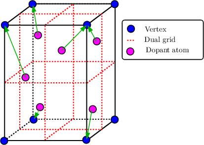
| Figure 5.2: | Illustration of the randomization algorithm, in a single cell, detailed in the text. The dual grid is shown in red. The green arrows depict the assignment of the dopants to the respective vertices. |
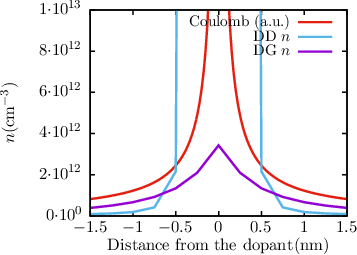
Considering single point charges in the numerical solution of the Poisson equation a problem emerges. Since the potential of a point charge located at r0 is qδ(r -r0), this would result in an infinite number of charge carriers screening the point charge (cf. Figure 5.3). Certainly this behavior is unphysical and an artifact of a classical or semi-classical system description, since the point charge serves as a potential well for charge carriers and thus can be screened by a few electrons or holes occupying discrete eigenenergies as described by the Schrödinger equation. Additionally, a semi-classical description of point charges is highly dependent on the grid spacing. Thus in a semi-classical system description correction methods are required. In the literature two approaches can be found to eliminate the artificial screening effect and to make the results of the simulation fairly independent of the grid spacing. In the first approach the Fourier transformed charge density of the point charge is calculated and formally split into a long range and a ‘short range’ part per finite volume i:
ρ(r) = qδ(r) = qV i-1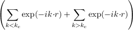 = ρshort(r) + ρlong(r), = ρshort(r) + ρlong(r), | (5.1) |
| kc = κN1∕3, | (5.2) |
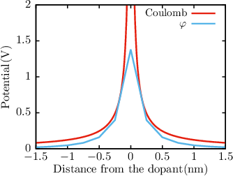
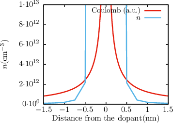
| Figure 5.3: | The potential ϕ (left figure) and the electron concentration n (right figure) around a single point charge embedded in pure silicon obtained by a DD or SHE simulation in equilibrium are shown. Without any correction of the coloumb potential a semi-classical simulator will predict an infinite amount of electrons around the point charge. |
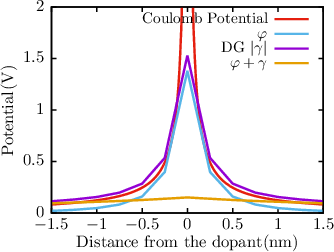
| Figure 5.4: | The potential ϕ (left figure) and the electron concentration n (right figure) around a single point charge embedded in pure silicon obtained by a quantum-corrected DD or SHE simulation in equilibrium are shown. A grid independent correction of the coloumb potential is achieved via the density gradient model, such that only the long range part ρlong(r) of the coloumb potential enters Poisson’s equation. In the figure γ denotes the quantum correction potential and ϕ + γ is the quantum corrected potential. |
The algorithms laid out in the sections before have been implemented into the simulator MinimosNT [90]. First, in order to investigate the grid dependence of the results, a simple n-type 10nm × 10nm × 100nm nanoscale resistor is simulated (cf. Figure 5.5 and Figure 5.6). Due to the fluctuations of the doping, the potential is expected to be spatially fluctuating as well, resulting in charge carrier rich and charge carrier deprived areas. This leads to fluctuations in device parameters (resistivity) from device to device, although macroscopically they are exactly the same. But due to the small characteristic lengths the doping cannot be viewed macroscopically. Thus hundreds of microscopically different devices have to be investigated in order to asses the inter-device distribution of parameters in any nano-scale devices.
| Figure 5.5: | The discrete doping in an n-doped 50nm long, 10nm times 10nm wide resistor with idealized ohmic contacts. The initial doping ND = 1020cm-3 concentration was assumed to be uniform. |
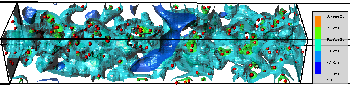
| Figure 5.6: | A surface plot of equal electron concentrations in equilibrium (all terminals are grounded). The simulation has been carried out at room temperature using MinimosNT. The dopant distribution is shown in Figure 5.5. The grid is orthogonal and regular with a spacing of 0.5nm. |
Upon investigation of the influence of random discrete dopants with the density gradient model as quantum correction for the drift diffusion model to a MOSFET a new effect emerges. In sub-100nm channel length MOSFETs, there are only few dopants in the channel leading to considerable potential fluctuations. Thus the inversion condition becomes a function of the spatial locations of the discrete dopants and leads to the formation to current percolation paths (cf. Figure 5.7). This in turn leads to substantial fluctuations in the Id - Vg-characteristic and consequently to fluctuations of the threshold voltage from device to device (cf. Figure 5.8).
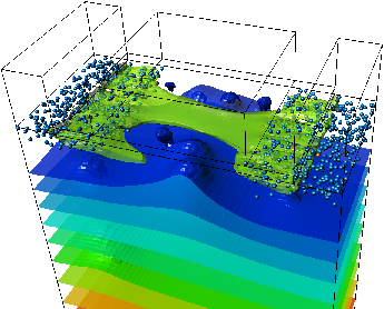
| Figure 5.7: | The percolation path (in green) in a MOSFET in weak inversion and equi-potential surfaces. Due to the potential fluctuations the conditions for charge carrier inversion is only fulfilled in certain regions of the channel, causing dominant current paths. Donor dopants are rendered as blue balls and acceptor dopants as golden balls. |
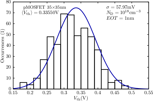
| Figure 5.8: | Histogram of the distribution of the threshold voltage in a MOSFET composed of 500 microscopically different devices. A Gaussian distribution of Vth has been fitted to the data. The standard deviation is above 30mV. In order to circumvent this large deviation in the threshold voltage the utilization of a delta-doping has been put forward [99]. |