Pseudomorphic HEMTs on GaAs substrates are now widely used for various applications in the frequency range from 0.9/1.9 GHz [65] up to 94 GHz [66, 67]. In all cases they are optimized for the given requirements. The applications can be divided into three categories which are characterized by the property of the HEMTs which are specifically optimized. In the following each category will be investigated by means of measurements and simulations.
The first investigated category are HEMTs for low noise applications which was the primer motivation for the development of the first HEMTs in 1980 [68, 69].
The second category is that of power HEMTs. The optimized parameters highly depend on the operation frequency. Presently two frequency bands are in the focus of interest. The lower band is around 0.9/1.9 GHz used for mobile communication where HEMTs are competing against various other technologies such as Si/GeHBTs, IIIVHBTs, and GaAs-MESFETs. Therefore cheap large volume production is one of the most important issues. These HEMTs typically have uncritical gate lengths between 500 nm and 1 µm and breakdown voltages of 10 V and higher. The upper band for power HEMT applications around 40 GHz is used for base stations. The main concern for the design of these HEMTs is the trade off between power capability and RF performance.
The third category are HEMTs for millimeter wave applications such as
collision avoidance radar at 77 GHz and military radar at 94 GHz. They
have to be optimized in first place with respect to their RF performance.
Therefore they typically exhibit gate lengths below 150 nm and breakdown
voltages in the order of 5 V.
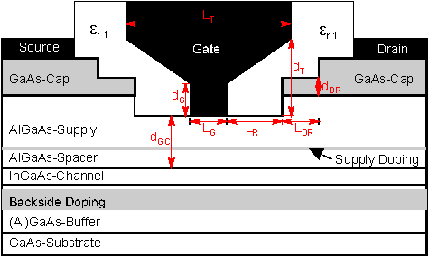
The figures of merit of a HEMT in first place are the transconductance
gm, the maximum drain current ID max,
the output conductance g0, the drain source breakdown
voltage VDS br, and the gate capacitances CGS
and CGD. The most important design parameters of HEMTs
are indicated in Figure
6.1. Besides the epitaxial layer thicknesses these are the gate to
channel separation dGC, the cap recess dDR,
the lateral dimensions LG, LR and LDR,
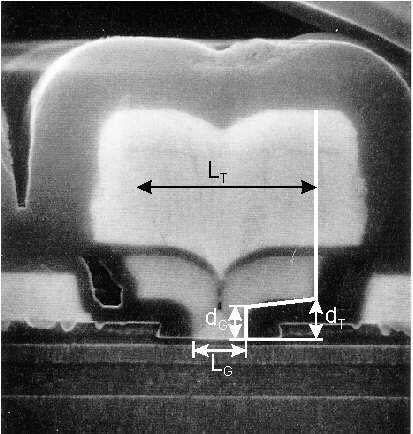
the passivation and the shape of the gate metal. The shape of the gate
is characterized by LG, LT, dT
and dG as shown in Figure
6.2.
To find the optimum design for given requirements not only a trade-off has to be made between various device characteristics but also such as between device performance and cost of production. One of the most expensive processing step of the HEMT is the definition of a small LG. Therefore, it is among the most important tasks to simulate the dependencies on LG accurately.
In the following sections about the three categories of HEMTs the capabilities
and the limitations of the simulator describing and optimizing the DC and
RF performance will be demonstrated. The investigation will be carried
out for VDS = 2.0 V if not stated differently to provide
good comparability between the various devices, although this is not the
optimum bias point for RF or power performance. The highest fT's
are usually reached for ![]() but the operating points are normally higher, especially for power applications.
As shown in the output characteristics in Figure
5.25 impact ionization which is not included in the simulation can
become significant for
but the operating points are normally higher, especially for power applications.
As shown in the output characteristics in Figure
5.25 impact ionization which is not included in the simulation can
become significant for ![]() .
Thus no higher voltage was chosen to compare simulation and measured results.
.
Thus no higher voltage was chosen to compare simulation and measured results.
All epitaxial layers of the HEMTs used for the investigations in this
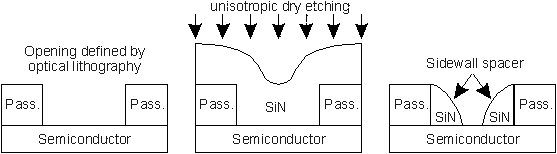
work are grown by molecular beam epitaxy (MBE). To define extremely small
gate structures optical wafer stepper lithography with phaseshift
masks is used. The obtained opening is reduced by a SiN sidewall spacer
process schematically shown in Figure
6.3. This process yields a characteristic shape of the gate cross section
shown in the SEM photograph in Figure
6.2. The typical rounding near the footprint of the gate can be controlled
by the spacer process.
This is different to the typical gate cross section obtained from a
multi layer resist electron beam lithography (EBL) as shown in Figure
6.4. EBL structures well below 100 nm can be defined in a photoresist
and directly transferred to the layers on the semiconductor [70].
Thus, relatively high distinct Tgate stems can be obtained.
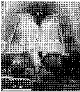
The major drawback of EBL is the very high cost and low throughput in the production compared to optical lithography. A benefit of the sidewall spacer technology is that the recess length LR and the gate length LG can be defined independently [72].
The approximation of the Tgate shape by LG, LT, dT and dG in the simulation does not have an influence on the DC characteristics of the device but leads to a certain error in the gate capacitances. The exact modeling of the Tgate shape is getting more important the smaller the distance between the gate metal and the highly doped cap and/or the drain metal. Unfortunately it is usually not possible to experimentally determine the exact Tgate shape of the actual measured device because the device has to be destroyed for the SEM photograph. Nevertheless, the influence of a change of the Tgate shape on the gate capacitances can be calculated very well by simulation.
In Section 6.1 three low noise HEMTs will be
investigated which posses the same epitaxial layers and differ only in
their geometry defined by the process technology. In Section
6.2 two power HEMTs are considered processed on the same wafer which
differs only in their gate lengths LG. The lateral spacings
are increased compared to HEMTref
for higher breakdown voltages. In Section 6.3
the optimization of HEMTref
for millimeter wave applications is described. Verifications of the simulated
results are carried out on two devices with different dGC.
In Section 6.4 general considerations about the
comparison of the different HEMTs are given.
Helmut Brech 1998-03-11