One of the most important figure of merit of a HEMT is the current-gain cutoff frequency fT given by (10) and fmax given by (11) as described in Chapter 3.
For the case of HEMT
A, Figure
6.13 shows a comparison of the functions fT (VGS)
determined in three different ways: i) measured (i. e., obtained by Sparameter
measurements), ii) calculated with (10)
where gmi, CGSi, and CGDi
were obtained from extractions using the small-signal equivalent network
shown in Figure
3.1, and iii) obtained from simulations also using (10)
with the approximation for the extrinsic values described in Chapter
3.
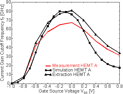
The last two cases offer the possibility to determine the device performance excluding the contacting network which is necessary for circuit design.
The maximum fT of the simulation was fitted to fT
max calculated with extracted small signal parameters by adjusting
the cross section of the Tgate. The smaller simulated fT's
below and above gm max reflect the underestimated electron
velocity due to the DD model in the GaAs and AlGaAs layers. The measured
maximum fT is about 13 GHz lower than the calculated
ones mainly due to the presence of the parasitic elements of the small
signal equivalent shown in Figure
3.1. The values of the small-signal circuit elements for HEMT
A obtained by parameter extraction, which are considered to be not
bias dependent, are given in Table
6.4.
|
|
|
|
|
|
|
|
|
|
|
|
|
|
|
|
In the following we want to examine the influence of the geometrical
parameters LG and LR on the magnitude
of fT and fmax simulated according
to (10) and (11),
respectively. The capacitances CGS and CGD
entering the equations are considerably influenced not only by LG
and LR but also by the shape of the gate metal cross
section (imagine, for instance, the case of a T-gate) and the dielectric
constant er of the passivation
material that fills the space between metal structure and semiconductor
surface. The simulator is able to take all these effects of surface topology
fully into account. On the other hand, only in simulation it is possible
to analyze the hypothetical case that the gate does not interact capacitively
with the surrounding semiconductor surfaces or with the neighboring ohmic
contacts. This can be achieved by choosing er
= 0 and leads to the determination of the theoretical maximum of fT
for given LG and LR.
Helmut Brech 1998-03-11