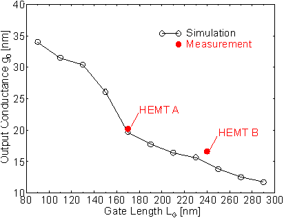
6.1.2.1 Reduction of the Gate
Length
When LG is reduced, fT will increase,
but a simultaneous and undesirable increase of the output conductance g0
must be expected due to short channel effects such as increased real space
transfer. In Figure
6.14 the simulated parameter g0 (at the bias point
VDS = 2 V, VGS = 0.2 V) is shown as
a function of LG and compared to the experimental DC
values of HEMTs
A and B
which differ only with respect to LG but not in any other
geometrical dimensions. The simulation is able to reproduce g0
realistically.
As described in Section 5.3.1, the increase of gm ext is only small when LG is reduced. The capacitance CGD is nearly independent of LG. The gate-source capacitance CGS is only partly dependent on LG: fringe and other parasitic contributions are independent of LG, only the part due to the gate contact area is length dependent. Therefore, the improvement of fT which can be achieved by a reduction of LG depends on the relative contribution of the parasitic (i. e. constant) part of the capacitance to the gate capacitance CG.
In Figure
6.15 the simulated fT is shown along with the measured
and deembedded fT according to the procedure described
in Section 3.2. Although only the simulation of
HEMT
A was fitted to the deembedded fT also the fT
of HEMT
B is simulated very well. The measured values in Figure
6.15 (which are taken from HEMTs
A and B)
are even below the ones calculated with complete T-gate structure and passivation
nitride due to the presence of parasitic pad capacitances as discussed
before.
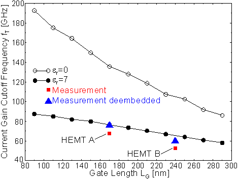
The dependence of fT on LG is shown in Figure 6.15 for two examples: the theoretical limiting case of er = 0 where the contribution of parasitics is reduced to the inevitable fringe capacitances at the gate edge, and the case of the presence of a medium with er = 7 (a silicon nitride passivation layer, for instance) which fills the space between the Tgate overhang and the semiconductor surface in the manner sketched in Figure 6.6. Figure 6.15 demonstrates clearly that the improvement of fT achieved by a reduction of LG depends strongly on the relative contribution of parasitic capacitive couplings to the total gate capacitance. The reduction of fT in the presence of passivation layers has been experimentally observed by Wu et al. [78].
To obtain an fT of 100 GHz, a fully passivated device
of the general structure of HEMT
A must be either supplied with a gate length below 100 nm, or the gate
length is left as large as in HEMT
B (240 nm) but no passivation is allowed at all. The case of an unpassivated
device in air with er = 1
is close to the idealized case er
= 0 plotted in Figure
6.15. The two curves in the Figure are calculated under the assumption
of a constant interface charge density which is certainly an idealization
when the unpassivated case is considered.
Helmut Brech 1998-03-11