6.2 Power HEMT for 0.9/1.9 GHz
and 40 GHz Applications
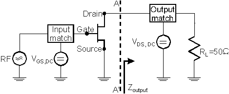
In contrast to small signal applications a large voltage swing is applied on HEMTs for power applications. To obtain high output power the devices have to sustain high voltages and high current densities. A principle amplifier circuit is shown in Figure 6.19. If the transistor is biased with a certain DC bias voltage VDS, DC and VGS is altered with low frequency a straight load line in the output characteristics occurs. The slope of the load line is defined by the load resistance.
However, as the frequency of the input signal increases the capacitive
and inductive elements of the transistor and the matching networks eventually
become significant. The voltages occurring on the transistor can be determined
by circuit simulation. In Figure
6.20 the output characteristics of HEMTref
is shown along with ID/VDS characteristics
in the plane AA' indicated in Figure
6.19 for a sinusoidal input signal with 38 GHz. For each cycle of the
input signal one corresponding ID/VDS
characteristics is covered. For the shown example HEMTref
is DC biased at VDS = 3.0V and VGS
= 0.35 V. The largest trajectory was obtained for an input voltage swing
of ![]() , the
smallest for
, the
smallest for ![]() .
.
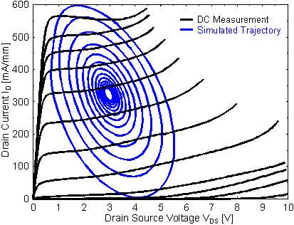
The trajectory is widened not only with the applied input voltage swing but also with increasing frequency, thus a much larger area of the output characteristics is covered than in the DC case. This increases the requirements for the devices used for high frequency applications substantially. Not only the source drain breakdown voltage Vbr for VGS near VT is important but also Vbr for high VGS is becoming increasingly crucial with increasing operation frequency.
As discussed in Section 5.3.2.2 different breakdown regimes can be identified in the output characteristics of a HEMT. In any case these are attributed to high electric fields in some regions of the device. In pseudomorphic HEMTs the most common breakdown occurs in the channel due to its small bandgap. Thus, investigations will focus on the dependences of various geometry parameters on the maximum electric field in the channel for different bias points. Besides breakdown the RF performance of the devices is equally important. The DC and RF properties will be investigated by means of simulation and measurements. The trade-off between RF performance and power capability will be addressed.
In Figure
6.21 a schematic cross section of the investigated power HEMT is shown.
The most significant changes from HEMTref
to power HEMTs investigated in this work are a smaller dGC,
larger lateral spacing LR, and an additionally recessed
cap layer to improve the breakdown voltage. To investigate the dependence
of the RF performance on the passivation thickness layer with two different
dielectric constants er1 =
1 and er2 = 7 are considered
in the simulation. In addition the influence of the Tgate shape on
CG will be investigated. To analyze this effect quantitatively
the gate geometry will be characterized by LT, LG,
dT, and dG as shown in Figure
6.1.
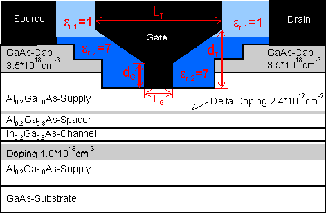
The low noise HEMTs investigated in the previous section and HEMTref
have self aligned contacts, i. e., the gate metal serves as a mask to define
source and drain contacts, thus LT is the source to drain
contact separation. This is different for the power HEMTs were LT
is smaller than the source to drain separation as depicted in the cross
section shown in Figure
6.21.
Helmut Brech 1998-03-11