The investigations are based on two power pseudomorphic HEMTs manufactured
on the same wafer which differ only in their gate lengths of LG
= 220 nm and 500 nm. The simulations are performed with the simulation
set up obtained by the fitting procedure on HEMTref.
The model parameters are given in Table
5.2 . First the simulation of the device with LG
= 220 nm was fitted to the measurements only by adjusting the location
and density of the active doping in the supply layer, the interface charge
density, and the gatetochannel separation. All adjustments are
made well within realistic ranges. Then the device with LG
= 500 nm was simulated with the same set of simulation parameters but the
corresponding lateral spacings.

The measurements and simulations of the transfer characteristics and
the transconductance gm of the two HEMTs are compared
in Figure
6.22 and Figure
6.23. Although only the simulation of the device with LG
= 220 nm was fitted to the measurements also the results for the device
with 500 nm agree very well.
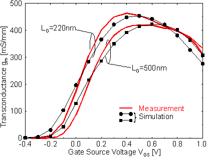
Again the current near VT is overestimated. Despite this small discrepancy it is shown in both the simulation and the measurements that VT differs by about 110 mV. The lower average electron velocity due to the longer gate manifests itself also in a reduction of gm as shown in Figure 6.23. A more positive VT and a lower gm results in a significantly lower ID max for the device with LG = 500 nm. However, there is also a small but important detail in which simulation and measurement do not agree completely. Although the simulated ID max for the device with LG = 220 nm is slightly underestimated the simulated ID max of the HEMT with LG = 500 nm is somewhat overestimated. A possible reason for this behavior can be explained as follows.
The current saturation for large VGS is mainly governed by real space transfer, the velocity in the barrier layers, and the interface charge density between the semiconductor and the passivation. The real space transfer and the velocity changes with the gate length but the interface charge density is kept constant. Thus, the relative impact of the interface charge density and the transport properties on the total current is changed with the gate length. The CG of HEMTref in Figure 5.22 revealed an underestimated carrier concentration and an overestimated carrier velocity for VGS > 0.6 V. This is obviously getting significant due to the change of the relative impact of the parameters. This is another indication that the discrepancy between measurement and simulation of HEMTref for VGS > 0.6 V is not solely due to thermal effects but also calls for improvements of the HD model for AlGaAs.
On the other hand the two devices already cover a very wide range of
technically relevant gate lengths, thus, based on the verification of the
simulation results the capability of predictive simulations can considered
to be very substantial.
Helmut Brech 1998-03-11