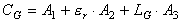
6.2.3.2 Contributions to the Gate
Capacitance
In order to identify the different contributions to CG,
we use the procedure described in Section 6.1.2.
The capacitive coupling of the gate metal to the ohmic contacts and to
the semiconductor material is minimized by setting er1
= er2 = er
= 1 (no passivation at all). The opposite extreme is represented by the
case er = 7. Figure
6.32 shows the simulated CG as a function of LG
for both cases. Again a linear fit can be found for CG
versus LG and also on er
which was demonstrated in Section 6.1.2:
 . . |
(62)
|
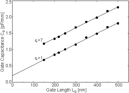
By extrapolation of the straight line for er = 1 to LG = 0, the fringe capacitance CF = A1 + A2 is obtained. In Figure 6.32, CF 200 fF/mm. From the separation of the two straight lines A2 can be deduced. In this case, A2 » 85 fF/mm. Finally, A3 = 3.2 nF/mm2 is given by the slope of the two lines. (for a gate with LG = 100 nm, this is equivalent to 320 fF/mm).
A1 and A3 depend on the epitaxial
layers, whereas ![]() is given by the geometry of the contacts and the permittivity of the dielectric.
In the following the influence of
is given by the geometry of the contacts and the permittivity of the dielectric.
In the following the influence of ![]() on the thickness of the passivation and the shape of the Tgate will
be investigated.
on the thickness of the passivation and the shape of the Tgate will
be investigated.
Helmut Brech 1998-03-11