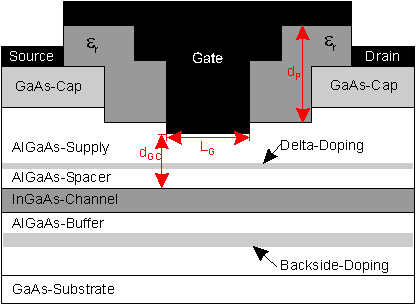
The basic structure of the investigated HEMT is shown in Figure
6.38. The epitaxial layers are similar to those of HEMTref.
In the barrier below the channel a 5 nm thick layer with a doping concentration
of 1.1*1018 cm3 is used. The upper barrier layer
contains a delta doping with a sheet concentration of 3.6*1012
cm2. The Tshaped gate with a footprint length LG
of 120 nm was manufactured by optical stepper lithography and a side wall
spacer process as the previous described HEMTs. Source and drain contacts
are selfaligned to the Tgate [72].
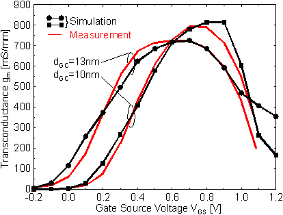
The verification of the simulation is based on two devices manufactured
on the same wafer. It was intended to create the same recess depth for
all devices. Inhomogenities in the etching process lead to some differences
in dGC. The devices are simulated using the setup and
model parameters obtained from HEMTref
in Section 5.3.2. A HD model is used in the
channel and supply layer and the DD model in the remaining semiconductor
layers. The simulated transfer characteristics were fitted to the measurements
of one device only by adjusting the given nominal values for the location
and density of the delta doping in the supply layer, the interface charge
density, and the gate-to-channel separation.
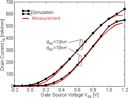
The measurements of both devices are shown in Figure
6.39. The simulation of the device with dGC = 13
nm was fitted to the measurement. Again the overestimation of the current
near VT is significant. Between VGS
= 0.4 V and VGS = 1.0 V simulation and measurement agree
very well whereas for higher VGS the deviations already
discussed in Section 5.3.2 and Section
6.2.1 occur. The second measurement can be simulated by a reduction
of dGC to 10 nm. Although the deviations are somewhat
larger than for the other simulation Figure6.40
shows that the change in gm is simulated very realistically.
Helmut Brech 1998-03-11