6.3.1.1 Dependence on the Gate-to-Channel
Separation
In Figure
6.41 gm max is shown over a wider range of dGC.
Within the accuracy of the simulation gm max is increased
linearly with about 28 mS/mm for a reduction of dGC by
1 nm. The simulations are performed under the assumption that the Schottky
barrier height FB is constant.
One has to expect a deteriorated FB
if the distance between the gate and the delta doping gets below a certain
value.
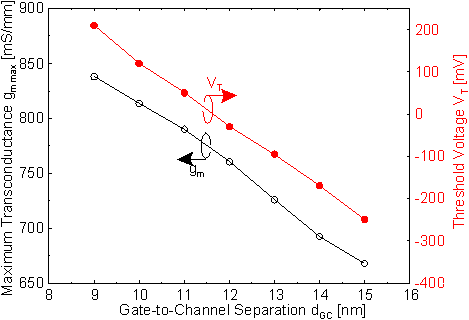
It is shown in Figure
6.41 that the threshold voltage VT is also very sensitive
to dGC. VT is shifted by about 75 mV
for a change of dGC of only 1 nm, thus very tight process
control is necessary to provide high uniformity over the wafer which is
an important requirement for digital ICs [81,
82]. A high
reproducibility even from one wafer to another is required for ICs with
only a positive bias voltage were only enhancement mode HEMTs can be used.
Helmut Brech 1998-03-11