6.3.1.2 Dependence on the Gate
Length
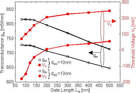
In Figure
6.42 VT is shown as a function of the gate length
LG for dGC = 10 nm and dGC
= 13 nm. In both cases only a moderate shift of about 1 mV has to be expected
for DLG = 10 nm and LG
> 200 nm. For LG = 100 nm and DLG
= 10 nm the expected shift for is 8 mV. The stronger shift for small LG
can be attributed to short channel effects which has also a significant
impact on the transconductance as shown in Figure
6.42. Below 200 nm the characteristics for both dGC
saturate whereas a linear reduction of gm is shown for
LG > 200 nm.
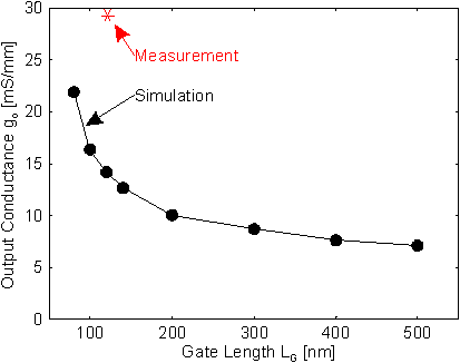
The most severe short channel effect is an increase of the output conductance
g0. In Figure
6.43 the simulated g0 is shown as a function of LG.
The measured value indicated by the asterisk is about two times higher.
One reason for the discrepancy is the use of the DD transport model in
the buffer layer. The second more important reason is that impact ionization
is not included in the simulation. It was shown in Section
5.3.2.2 that impact ionization is already significant for VDS
> 2.0 V for HEMTref.
The millimeter wave HEMT presented in this section exhibits significantly
smaller lateral dimensions thus an increase in g0 due
to impact ionization has to be expected for even smaller values of VDS.
Despite the underestimated magnitude of g0 the principle
characteristics of g0 is simulated realistically. The
output conductance is almost doubled if LG is reduced
from LG = 140 nm to 80 nm.
The presented results on the DC performance shows an improvement of
gm by more than 50 % compared to the gm
of the power HEMT of Section 6.2.
Helmut Brech 1998-03-11