6.3.2.5 Dependence on the Passivation
Thickness
In Figure
6.49 fT and fmax are shown as a
function of the thickness of the passivation dP. The
ideal case was assumed that the DC characteristics of the device would
not deteriorate by reducing or even removing the passivation.
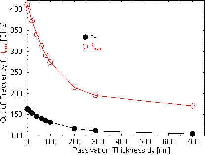
fT is increased from 104 GHz for a fully passivated
device to fT = 163 GHz for an unpassivated one. fmax
increases accordingly from 170 GHz to over 400 GHz. It was shown in Section
6.2.3.3 for the power HEMTs that the electric field is rather low at
the top of the passivation and increases significantly towards the gate
edge. Therefore only a minor improvement shown for a reduction in dP
from 700 nm until the surface of the passivation reaches the semiconductor
interface.
Helmut Brech 1998-03-11