As an example, consider the long channel nMOSFET shown in Figure 5.1, operating in inversion mode. We assume no recombination and stationary conditions. No voltage is connected between source and drain, and therefore the device is current-free. To compensate the electric field in the channel arising from the applied gate voltage, a carrier displacement will occur in that area.
The set of equations are the Poisson equation and the semiconductor equations
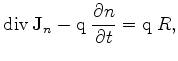 |
(5.2) |
 |
(5.3) |
| (5.4) | |
| (5.5) |
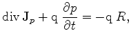
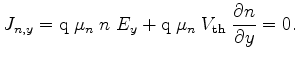
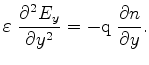
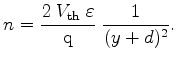
In inversion mode, the holes under the gate are displaced and the following relation holds
 |
(5.12) |
 |
(5.13) |
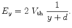 |
(5.14) |
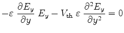
Here it can be seen that the electric field and even more, the carrier concentration changes rapidly along the y-axis, whereas along the x-axis the values remain unchanged. In Figure 5.2 the resulting carrier concentration of such a device is shown. Here the silicon segment has a constant donor background doping of
![]() and the highly doped areas under the source and drain contacts have a constant acceptor doping of
and the highly doped areas under the source and drain contacts have a constant acceptor doping of
![]() . The oxide thickness under the gate contact is 20 nm. By applying a drain-source voltage and without a gate-source voltage, one of the two source/silicon or drain/silicon pn-junctions are in reverse direction and the device is blocked.
With a gate bias of 10 V and all other contacts grounded, the carrier concentrations raise at the gate regions. The device is in inversion and the carrier concentrations under the gate contact are higher than the concentrations in the source and drain regions. The pn-junctions are not reverse biased any longer.
. The oxide thickness under the gate contact is 20 nm. By applying a drain-source voltage and without a gate-source voltage, one of the two source/silicon or drain/silicon pn-junctions are in reverse direction and the device is blocked.
With a gate bias of 10 V and all other contacts grounded, the carrier concentrations raise at the gate regions. The device is in inversion and the carrier concentrations under the gate contact are higher than the concentrations in the source and drain regions. The pn-junctions are not reverse biased any longer.
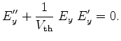
With introducing a voltage between source and drain, a current will arise. As the free charge carriers are responsible for the current density, a relatively high current density change along the y-axis, combined with nearly constant current density along the x-axis will follow. In Figure 5.1, the current density, with a voltage of 1 V between source and drain, is shown. Along the channel, the current density is almost constant.
This simple device with planar silicon surfaces has been simulated based on an ortho grid.
The comparison of different grid approaches, with a dense grid with a grid spacing of 0.01 nm along the y-axis and a coarse grid with minimum grid distance of 20 nm under the gate, and the result of the analytical solution is shown in Figure 5.1. The analytical solution loses its validity since relation (5.6) is violated. Comparing the simulations, an underestimation of the current density under the gate contact of about ![]() can be detected, which may decide about an breakdown of the device in critical cases.
can be detected, which may decide about an breakdown of the device in critical cases.
![\includegraphics[width=11cm]{ex1/carrier2}](img465.png)
|
![\includegraphics[width=13cm]{ex1/gnu}](img467.png)
|
![\includegraphics[width=12cm]{picsconveps/mos.eps}](img439.png)
![\includegraphics[width=11cm]{ex1/current2}](img466.png)