To retain adequate electrostatic control of the conduction channel in a transistor, different architectures, finFETs or UTB-SOI structures are used. The increased surface-to-volume ratio in these architectures has made the effects of scattering due to surface roughness between material interfaces a significant factor in the electrical performance. Surface scattering is now one of the dominant scattering mechanisms in devices with quasi-ballistic transport.
Interface roughness can be modelled by adding random perturbations to a smooth interface. The perturbations are statistically characterized by an autocorrelation function with parameters signifying the mean offset and the correlation length. Measurements have revealed that Si/SiO2 interfaces can be characterized by an exponential autocorrelation function with a variance and a correlation length. The mean offset can range between 0.1nm and 0.3nm for a Si/SiO2 interface [165, 166].
A numerical synthesis of the one-dimensional roughness, exhibiting the desired statistical properties, can be obtained by first generating a sequence of (uncorrelated) random numbers, which is then convolved with a impulse response (to be chosen) such that a random number sequence is produced with the desired degree of correlation. The Wiener-Kinchin theorem states that the spectral components of an autocorrelation function are given by the power spectral density (PSD) of the sequence used to obtain said function:

 has a PSD of an exponential autocorrelation function. Since rxx is generated, its PSD is known (or can be calculated); the transfer function
H
has a PSD of an exponential autocorrelation function. Since rxx is generated, its PSD is known (or can be calculated); the transfer function
H =
=  , such that
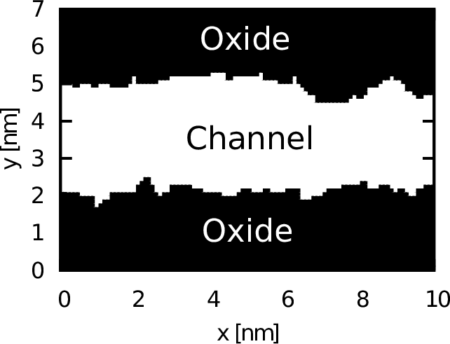
A sequence of perturbations  is generated by which the ideal (smooth) interface is displaced. Figure C.1 shows an example of a roughened interface
with the parameters given in the caption. To appropriately resolve such perturbations requires a very fine spatial resolution for the potential
profile. The latter leads to very high memory demands for the annihilation algorithm, which can be handled by the algorithms presented in the
Section 4.3.
is generated by which the ideal (smooth) interface is displaced. Figure C.1 shows an example of a roughened interface
with the parameters given in the caption. To appropriately resolve such perturbations requires a very fine spatial resolution for the potential
profile. The latter leads to very high memory demands for the annihilation algorithm, which can be handled by the algorithms presented in the
Section 4.3.