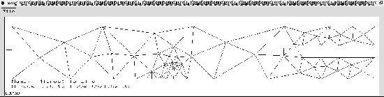
Figure 8.5: Geometry of a four-conductor problem
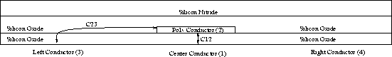
Fig. 8.5 shows the geometry of a four-conductor problem consisting of a central polysilicon conductor embedded in a silicondioxide segment which is contacted by three bottom boundary conductors. The central variable-width boundary contact forms, together with the polysilicon conductor, a microstrip line which is framed by the other two bottom contacts of constant width. The whole structure is covered by a silicon-nitride segment on its top.
The design goal is to find a certain width for the central bottom contact such that the parasitic capacitance of either of the two outer bottom contacts against the polysilicon conductor is less than one percent of the capacitance of the microstrip line itself. Therefore

must hold. The whole structure has an overall width of  and a height
of
and a height
of  . The central polysilicon conductor has a width and height of
  and
and  , respectively, whereas the outer bottom contacts are
 wide. A constant gap of
  is held between the central and
the outer bottom contacts.
is held between the central and
the outer bottom contacts.
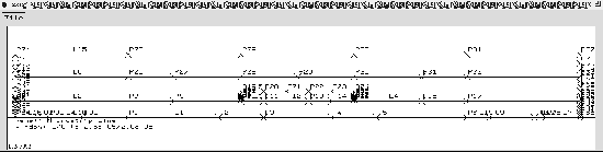
Figure 8.6: Example input data
In order to find now the proper width of the central bottom contact where the
capacitance relation stated above is fulfilled, this width is now varied from
 to
to  in
in  increments for the capacitance
calculations with VLSICAP. Therefore five VLSICAP runs have to be
performed, where the respective coordinates of the boundary points of the left
and central conductor are varied accordingly.
increments for the capacitance
calculations with VLSICAP. Therefore five VLSICAP runs have to be
performed, where the respective coordinates of the boundary points of the left
and central conductor are varied accordingly.
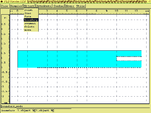
Figure 8.7: VLSICAP example edited with PED
Since the problem is symmetric, it is sufficient to simulate only
one half of the structure. Furthermore, the upper silicon-nitride segment's
influence on the capacitances is negligible, which can therefore be omitted in
the geometry definition. Fig. 8.7 shows the geometry structure
edited with PED, which was finally used for the simulations. The resulting
capacitance  has to be doubled to account for the halving of the
central microstrip line.
has to be doubled to account for the halving of the
central microstrip line.
MESHCP and VLSICP are now run for each of the five resulting input
cases. Fig. 8.8 shows one of the resulting grids produced by
MESHCP. Note that due to the small gap of between
the lower contacts compared to the dimensions of the rest of the structured,
the grid generated is quite dense in this area, whereas relatively large
triangles are generated where the boundary point distances are larger. Since
MESHCP takes care of a smooth grid by not allowing rapid variations of the
area of adjacent triangles, this small gap results in a very small triangle
directly located at the boundary with the neighbouring triangles gradually
adapting to the coarser grid in the rest of the structure. This grid density
adaption criterion even at the mesh generation phase helps that the numerics
processor VLSICP is able to compute a solution with less necessary grid
refinements.
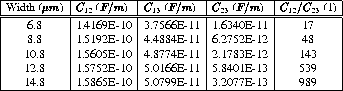
Figure 8.9: Table of the calculated capacitances
Fig. 8.9 lists the calculated capacitances ,
 and the ratio
  for the respective bottom contact
widths. The capacitance
for the respective bottom contact
widths. The capacitance  is just listed for completeness. As we can
see, a width of
is just listed for completeness. As we can
see, a width of  for the central bottom contact already fulfills
the requirement of a parasitic capacitance smaller than one
percent. Note that due to the constant distance of the lower contact from the
central polysilicon line, the respective capacitance remains almost
constant, whereas the capacitance between the central line and the left outer
contact varies considerably and decreases with increasing distance.
for the central bottom contact already fulfills
the requirement of a parasitic capacitance smaller than one
percent. Note that due to the constant distance of the lower contact from the
central polysilicon line, the respective capacitance remains almost
constant, whereas the capacitance between the central line and the left outer
contact varies considerably and decreases with increasing distance.