2. Silicon Oxidation Techniques
Oxidation is a process by which a metal or semiconductor is converted to an oxide. Although oxidation of many
materials plays a role in technology, the main oxidation reaction which will be addressed is the conversion of
parts of a silicon semiconductor wafer into silicon dioxide (SiO ). The chemical reaction between oxygen and silicon
to generate SiO is usually driven by a high-heat environment; however, even at room temperature, a shallow
layer of native oxide, approximately 1nm thick can form in an air environment. In order to grow thicker
oxides in a controled environment, several methods can be implemented:
). The chemical reaction between oxygen and silicon
to generate SiO is usually driven by a high-heat environment; however, even at room temperature, a shallow
layer of native oxide, approximately 1nm thick can form in an air environment. In order to grow thicker
oxides in a controled environment, several methods can be implemented:
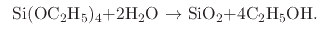
- Plasma Enhanced Chemical Vapor Deposition (PECVD) using TEOS as a precursor
is one way by which silicon dioxide can be grown on a silicon wafer [22]. This method is mainly used to grow a pad/buffer
oxide layer during LOCOS [131]. The reaction which takes place during PECVD using TEOS is
 |
(24) |
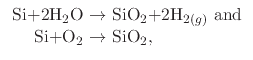
- Thermal oxidation of silicon surfaces is usually performed at high temperatures (800
 C - 1200
C), resulting
in a High Temperature Oxide (HTO) layer. The ambient environment can either be ``wet'' using water vapor or steam, or
``dry'' using molecular oxygen as the main oxidant. The reactions which take place during wet and dry thermal oxidation are
C - 1200
C), resulting
in a High Temperature Oxide (HTO) layer. The ambient environment can either be ``wet'' using water vapor or steam, or
``dry'' using molecular oxygen as the main oxidant. The reactions which take place during wet and dry thermal oxidation are
 |
(25) |
respectively.
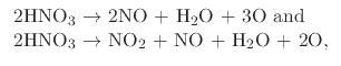
- Nitric Acid Oxidation of Silicon (NAOS) is performed at low temperatures (200
C - 400
C) and is used in order
to grow thin (1.3nm - 1.4nm) oxide structures. Similar to thermal oxidation, NAOS can be performed in liquid or vapor
environments. The chemical reactions which take place during wet and vapor NAOS are
 |
(26) |
respectively.
The different uses for thermally grown versus deposited oxides are laid out in Figure 2.1 [175].
Figure 2.1:
Difference in uses of thermally grown versus deposited silicon dioxide in silicon technology.
|
![\includegraphics[width=0.65\linewidth]{chapter_oxidation/figures/thicknesses.eps}](img131.png) |
Silicon dioxide layers are mainly used as high quality insulators or masks for ion implantation and the ability to form high
quality silicon dioxide is the main reason why silicon is still the dominating material for IC fabrication [175].
This chapter also introduces a novel technique for localized silicon oxidation, which allows nanosized oxide patterns to
be grown on a silicon surface far smaller than those available through traditional photolithography and electron beam lithography techniques.
The technique Local Oxidation Nanolithography (LON), also known as AFM-induced oxidation or Local Anodic Oxidation (LAO), uses the charged needle tip of an AFM
in order to generate the desired patterns.
Subsections
L. Filipovic: Topography Simulation of Novel Processing Techniques