Next: 3.4.3 Nanodot Modeling Using Up: 3.4 Local Oxidation Nanolithography Previous: 3.4.1 AFM Oxidation Mechanism
Empirical Models for LON started with the initial attempt to understand the physical mechanisms by Gordon et al. [65].
Teuschler et al. [123], [210] in the same year suggested that the height of the generated nanodot
is proportional to the ![]() root of the pulse time, (
root of the pulse time, (
![]() ). Although this empirical power law was a good fit to the
experimental data, there was no relation to the traditional idea of oxide growth models, such as those mentioned in
Chapter 2.
The first model based on the physical interactions during LON was introduced in 1997 by Stievenard et al. [197].
After analyses were done with thick oxides [4], it was found that a logarithmic time dependence of
). Although this empirical power law was a good fit to the
experimental data, there was no relation to the traditional idea of oxide growth models, such as those mentioned in
Chapter 2.
The first model based on the physical interactions during LON was introduced in 1997 by Stievenard et al. [197].
After analyses were done with thick oxides [4], it was found that a logarithmic time dependence of ![]() versus
versus ![]() is a good fit to the available experimental data with
is a good fit to the available experimental data with ![]() ranging from 0.01 to 1000s and
ranging from 0.01 to 1000s and ![]() up to 50nm. More refined models
for ICM-AFM and NCM-AFM lithographies were later suggested by Snow et al. [192] and Calleja et al. [28], respectively.
The models are for relatively thin oxides and pulse voltages below 30V, while for oxides grown under very high
voltage (30 to 50V), the Faradic current, which is present in the water meniscus, turns to ohmic current, and an additional
ring of oxide is grown along the outside of the nanodot [135]. These structures, grown under very high voltage,
are beyond the scope of the models presented in this work, but similar methods may be used in the future in order to include such
features in LON simulations.
up to 50nm. More refined models
for ICM-AFM and NCM-AFM lithographies were later suggested by Snow et al. [192] and Calleja et al. [28], respectively.
The models are for relatively thin oxides and pulse voltages below 30V, while for oxides grown under very high
voltage (30 to 50V), the Faradic current, which is present in the water meniscus, turns to ohmic current, and an additional
ring of oxide is grown along the outside of the nanodot [135]. These structures, grown under very high voltage,
are beyond the scope of the models presented in this work, but similar methods may be used in the future in order to include such
features in LON simulations.
|
Three types of AFM tip shapes have been analyzed in the literature [45]. The different shapes are for a rough, hemispherical, and blunt tip configuration, which can be modeled using a ring charge, point charge, and ring charge, respectively. We present two models: one for a hemispherical tip shape, which involves only one charged dot and one for all other tip shapes, where multiple charged dots are required in order to model the needle tip. The schematics of this approach are shown in Figure 3.11a and Figure 3.11b, valid for a hemispherical and blunt needle tip, respectively. For the implemented model, it is assumed that all oxyanions are generated at the effective point source of the AFM needle tip. This simplifies the model, while not having a significant consequence on the model's accuracy [164]. The oxyanions traverse through the water meniscus along electric field lines, finally colliding with the sample surface, whose evolution is visualized using the LS method [50], [51].
Using the method of image charges, the voltage and electric field strength in the water meniscus region has been calculated [149], [164]. The effects of surrounding ions on the electric field strength and recombination reactions between ions to form water were neglected [45]. Mesa et al. [149] suggest that each AFM needle can be represented as a series of charged particles distributed along the structure of the needle. The presented model implements this idea with the use of point charges, which is valid for all types of AFM needles.
As discussed in the previous section, the model representing the shape of a hemispherical AFM
generated nanodot follows the Surface Charge Density (SCD) distribution, which is derived by replacing the AFM
needle tip with an effective point source ![]() and the silicon substrate surface by an
infinitely long conducting plane. The image charge method is then applied to find the
voltage at every location in the water meniscus region
and the silicon substrate surface by an
infinitely long conducting plane. The image charge method is then applied to find the
voltage at every location in the water meniscus region
![]() :
:
![$\displaystyle {V\left(\vec{p}\right)=k\,Q\left[\cfrac{1}{\left(x^{2}+y^{2}+\lef...
...{1/2}}-\cfrac{1}{\left(x^{2}+y^{2}+\left(z+D\right)^{2}\right)^{1/2}}\right]} ,$](img417.png) |
(105) |
As mentioned in Section 3.4, in order to simulate the nanodot growth, initiated using a rough AFM tip, the needle may be modeled as a ring of charges at a given height above the silicon surface. The ring of charges is modeled by a desired number of dot charges surrounding the AFM tip circumference. When multiple dot charges are used to represent the AFM needle, the equation for the surface charge density becomes
There are not many models for LON with a scanning tunneling microscope. The reason for this is that, quickly after the discovery of STM
nano-oxidation, the AFM was introduced and shown to be a better tool for LON. The limitations of STM lithography when compared to AFM lithography are
higher tip degradation due to reduced conductivity, difficulty in evaluating the exact lithography after printing due
to the STM's inability to distinguish SiO![]() from the ambient, slow dip velocity required for stable
operation, and the requirement for STM to be operated in UHV [46].
An analysis of STM-induced oxidation was performed by Kramer et al. [108], [109],
which indicated that oxidation is induced by the electrical field between the tip and silicon sample and not by the
energetic electrons from the tip directly. With decreasing Relative Air Humidity (RAH), the generated oxide also decreases
in size, down to a threshold humidity of 10%, beyond which, no oxidation takes place [109]. Increasing the
applied reverse bias voltage also increases the oxide size, in both height and width. However, it is shown that the
inverse oxide line width has a logarithmic influence from the applied bias, as seen in Figure 3.12, which is
a reproduction of Figure 3 from [109].
from the ambient, slow dip velocity required for stable
operation, and the requirement for STM to be operated in UHV [46].
An analysis of STM-induced oxidation was performed by Kramer et al. [108], [109],
which indicated that oxidation is induced by the electrical field between the tip and silicon sample and not by the
energetic electrons from the tip directly. With decreasing Relative Air Humidity (RAH), the generated oxide also decreases
in size, down to a threshold humidity of 10%, beyond which, no oxidation takes place [109]. Increasing the
applied reverse bias voltage also increases the oxide size, in both height and width. However, it is shown that the
inverse oxide line width has a logarithmic influence from the applied bias, as seen in Figure 3.12, which is
a reproduction of Figure 3 from [109].
![\includegraphics[width=0.5\linewidth]{chapter_process_modeling/figures/STM_model.eps}](img429.png) |
The first physical-based model for CM nano-oxidation with an AFM was suggested by Stievenard et al. [197]. The model is based on
the Cabrera and Mott model and it suggests a linear relation between the oxide height (![]() ) and bias voltage (
) and bias voltage (![]() ) and a logarithmic
relationship between
) and a logarithmic
relationship between ![]() and
and ![]() ,
,
![]() . Another model, which shows the same patterns as those presented
in [197] is shown in [46].
Both models assumed a static RAH, with Stievenard's model setting it to 70%. This is ignored as a parameter; however, it
is well known that the amount of water which is available during oxidation influences the growth rate and size of the
oxide pattern [53].
. Another model, which shows the same patterns as those presented
in [197] is shown in [46].
Both models assumed a static RAH, with Stievenard's model setting it to 70%. This is ignored as a parameter; however, it
is well known that the amount of water which is available during oxidation influences the growth rate and size of the
oxide pattern [53].
From the initial assumption that the oxidation reaction is similar to the Cabrera and Mott model, but adapted for very thin oxide films, a model is developed in [197]:
If ![]() is the energy which an ion must overcome to diffuse, the kinetics of growth can then be given by:
is the energy which an ion must overcome to diffuse, the kinetics of growth can then be given by:
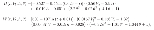
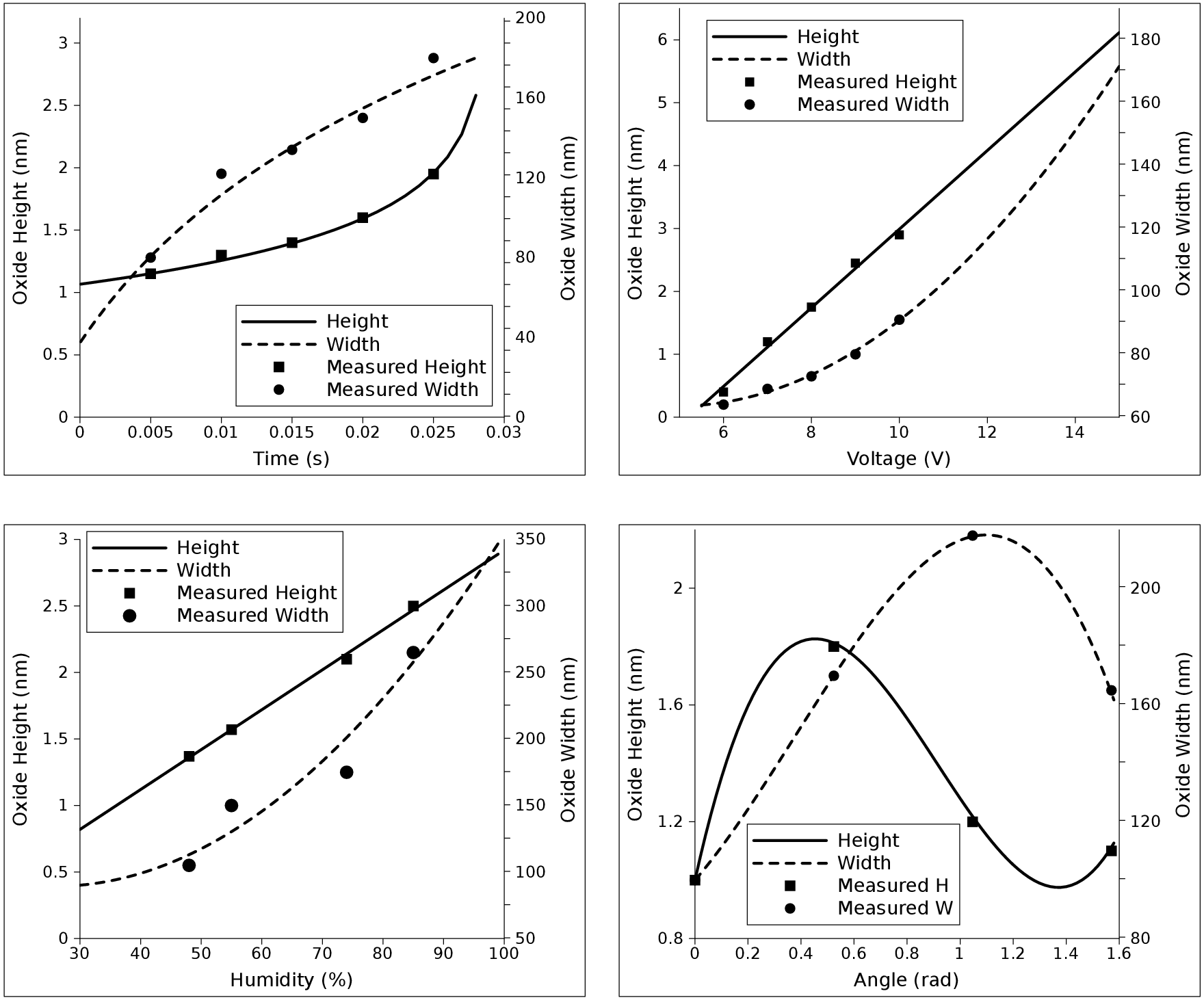
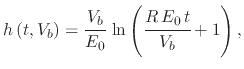
In order to simulate oxidation patterns using an AFM operating in ICM, the model presented in [192] is implemented. The equation which governs the height of the grown oxide is given by
The simulator also requires a dependence relationship for the Full Width at Half Maximum (FWHM) of the grown oxide, which is required in order to be able to generate a complete oxide nanodot. The work presented in [192] provides some measured results, shown in Figure 3.14. An empirical equation for the FWHM developed to fit the measured results is
 |
(116) |
![\includegraphics[width=0.65\linewidth]{chapter_process_modeling/figures/snowheight.eps}](img454.png) |
![\includegraphics[width=0.65\linewidth]{chapter_process_modeling/figures/snowwidth.eps}](img455.png) |
When operating the AFM in NCM mode, the formation of a field-induced liquid bridge is required in order to
provide oxyanions (OH![]() , O
, O![]() ), used to form the oxide. The liquid bridge also limits the
lateral extensions of the region to be oxidized. The model, implemented
in the process simulator, is described in [28], where it is suggested that
the width and height of a produced pattern have a linear dependence on the applied bias voltage,
while a logarithmic dependence exists for the pulse duration.
), used to form the oxide. The liquid bridge also limits the
lateral extensions of the region to be oxidized. The model, implemented
in the process simulator, is described in [28], where it is suggested that
the width and height of a produced pattern have a linear dependence on the applied bias voltage,
while a logarithmic dependence exists for the pulse duration.
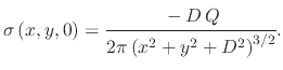
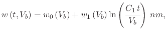
The empirical equation which governs the height of the oxide dot, produced using NCM, and presented in [28] is
 |
(118) |
 |
(120) |
![\includegraphics[width=\linewidth]{chapter_process_modeling/figures/calleja3.eps}](img460.png) |
In [53] the effect of humidity on the nanodot size is presented and the relationship is shown in Figure 3.16. A nearly linear relationship between humidity and the nanodot height is seen, while the width increases more rapidly, when the humidity is increased to 90%. This can be explained by the increase in water meniscus size with increased humidity, which provides more oxyanions to take part in the oxidation reaction.
The derived empirical equation which describes the effect of all three parameters (time, voltage, and humidity) on the height and width of the oxide dot in nanometers, produced using the AFM in NCM is given by:
In addition to using experimental observations in order to implement an empirical model for nanodots in the LS
simulator, the simulator has also been extended to include the generation of nanowires using an AFM in NCM. Although a nanowire can be
generated using a sequence of nanodots placed such that the lateral distance between each
dot is smaller than a dot's width, having a separate model for nanowires can help to speed up simulation times.
Simulating a nanowire as a sequence of nanodots means that each nanodot needs its own simulation step, while
having a single empirical equation which governs nanowire generation requires only one simulation step.
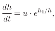
From the experimental results found in [53], relevant information is extracted in order to include the
effects on the nanowire shape due to variations in applied voltage, oxidation time, RAH, and wire
orientation, shown in Figure 3.17. The wire orientation is represented as an angle, where the (010) direction
is 0
![]() while (100) is 90
while (100) is 90
![]() for a Si (100) sample, shown in Figure 3.18 and Table 3.1.
for a Si (100) sample, shown in Figure 3.18 and Table 3.1.
|
 |
![\includegraphics[width=0.65\linewidth]{chapter_process_modeling/figures/Orientation.eps}](img468.png) |
It is evident that increasing the oxidation time,
the applied voltage, or the RAH results in an increased nanowire height and width. However, the effect
of the wire orientation is less predictable.
The smallest nanowire is noted at an orientation of
![]() , while the largest nanowire height is noted at
, while the largest nanowire height is noted at
![]() and
the largest FWHM is noted at
and
the largest FWHM is noted at
![]() . The effect of the wire
orientation on the height and width of the nanowire is not identical. The empirical equation, derived using the experimental results
from [53] and implemented in the LS simulator is given by
. The effect of the wire
orientation on the height and width of the nanowire is not identical. The empirical equation, derived using the experimental results
from [53] and implemented in the LS simulator is given by
In Figure 3.17 the results of the empirical equation (3.51) generated for this work are compared to the experimental data from [53].
![\includegraphics[width=0.481\linewidth]{chapter_process_modeling/figures/AFM_dotcharge.eps}](img414.png)
![\includegraphics[width=0.481\linewidth]{chapter_process_modeling/figures/AFM_ringcharge.eps}](img415.png)
![\begin{displaymath}\begin{array}{l} E_{x}=kQ\left[\cfrac{x}{\left(x^{2}+y^{2}+\l...
...{2}+y^{2}+\left(z+D\right)^{2}\right)^{3/2}}\right] \end{array}\end{displaymath}](img421.png)
![$\displaystyle \sigma\left(x,y,0\right)=-\cfrac{D}{2\pi}\overset{N}{\underset{i=...
...}{\left[\left(x-x_{i}\right)^{2}+\left(y-y_{i}\right)^{2}+D^{2}\right]^{3/2}} ,$](img424.png)
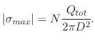

![\includegraphics[width=0.65\linewidth]{chapter_process_modeling/figures/OxideDot_humidity.eps}](img461.png)
![$\displaystyle \begin{tabular}{rl} $H(t,V_{b},h)=$\ & $\left[h_{0}\left(V_{b}\ri...
...left(V_{b}\right)\ln(t)\right]\cdot\left[0.019\, h-0.051\right]$, \end{tabular}$](img462.png)