5.2.1 Carbon Fluorides for Silicon Dioxide Etching
When modeling the plasma etching of silicon dioxide, it is important to include microloading phenomena which cause tapered vertical walls on the
etched SiO profile [151]. The tapering is caused by a polymer depositing on the well walls during the etching process. For example,
when SiO is etched using CF
profile [151]. The tapering is caused by a polymer depositing on the well walls during the etching process. For example,
when SiO is etched using CF gas, the CF gas undergoes a gas phase reaction, where it breaks into CF gas and F atoms. The CF gas
then undergoes a surface deposition reaction with the SiO. In order to simulate this phenomenon in the presented LS framework,
a model from [113] is implemented. It deals with an etching process with a simple chemistry such as a pure CF etch of SiO under
Ar
gas, the CF gas undergoes a gas phase reaction, where it breaks into CF gas and F atoms. The CF gas
then undergoes a surface deposition reaction with the SiO. In order to simulate this phenomenon in the presented LS framework,
a model from [113] is implemented. It deals with an etching process with a simple chemistry such as a pure CF etch of SiO under
Ar bombardment and polymer inhibition. The model parameters and constants which are implemented here can be found in [113].
The model suggests three surface coverages, one for the etchant
 , one for the polymer
 ,
and one for the active sites on the polymer coverage
,
and one for the active sites on the polymer coverage
 . The coverages are found using
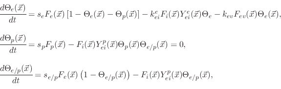 |
(194) |
where
 ,
,
 , and
, and
 are the total fluxes of the ion, etchant, and polymer, respectively and
 is an evaporation flux which is proportional to
 and temperature dependent. The constants
  ,
,  , and
, and  are the sticking coefficients of the etchant on SiO, polymer on SiO, and etchant
on the deposited polymer, respectively.
are the sticking coefficients of the etchant on SiO, polymer on SiO, and etchant
on the deposited polymer, respectively.
 and
and
 are etching yield functions.
Assuming steady state conditions, (5.35) can be used to find the surface coverages for each particle species
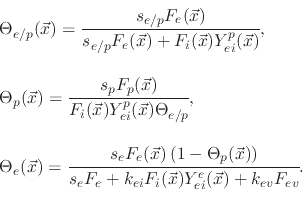 |
(195) |
The deposition rate of the polymer gas onto the wafer surface is given by the polymer flux and the sticking coefficient
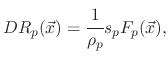 |
(196) |
where  is the polymer bulk density. The polymer can also be etched and this rate is given by the chemical sputtering rate
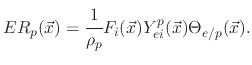 |
(197) |
If the polymer deposition rate is higher than its etch rate, then no etching on the surface occurs, but rather a deposition whose rate is
given by
 |
(198) |
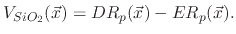
However, if the polymer deposition rate is lower than its etch rate, the film etching rate is given by
![$\displaystyle V_{SiO_{2}}(\vec{x})=-\cfrac{1}{\rho_{SiO_{2}}}\left[F_{i}(\vec{x...
...(\vec{x})
\left(1-\Theta_{e}(\vec{x})\right)+F_{ev}\Theta_{e}(\vec{x})\right],$](img712.png) |
(199) |
where
 is the SiO bulk density and
 accounts for the sputter yield of the silicon dioxide which is not covered by the etchant.
The threshold yield functions
depend on the ion energies and the impact direction of the ions onto the surface. In the case of physical sputtering, the yield is given by
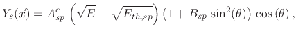 |
(200) |
where  is the impact angle,
  is the sputtering threshold energy,
  is the ion impact energy, and
  is a sputtering yield
factor. For ion enhanced chemical etching, the yield function is given by
is a sputtering yield
factor. For ion enhanced chemical etching, the yield function is given by
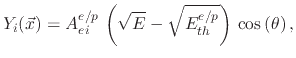 |
(201) |
where
 is the threshold energy and
 the etchant yield factor for ion enhanced chemical etching.
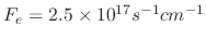
Figure 5.6 shows a simulation of the silicon dioxide etching process when various ion, etchant, and polymer fluxes are used. It is clear
that the ratio of etchant to polymer flux will decide how much polymer will be present on the sidewalls. Therefore, as the amount of polymer is decreased
with respect to the amount of etchant, shown from Figure 5.6a to 5.6c, the sidewalls show an increasing vertical
profile and higher etch rates. The simulation is performed through a 300nm diameter hole with an ideal mask for 80s. The profile is shown at 2s intervals.
This means that when etching the silicon dioxide layers for BiCS memory holes, an etchant should be used which produces
less deposition-inducing byproducts. When using CF , which was the etching process described in [113], the ratio of etchant to
polymer inhibitor flux is shown to be 2.5:1.
, which was the etching process described in [113], the ratio of etchant to
polymer inhibitor flux is shown to be 2.5:1.
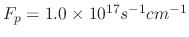
The ratio of etchant to polymer flux is not the only process parameter governing the final etched profile. Another important factor is the sticking
coefficient of the inhibitor species. The process described by the model in [113] suggests a sticking probability of 0.26. However, it would be
beneficial for a process with a lower sticking probability to be used when sharp vertical etch profiles are required.
In [86]
a process using CF is suggested for SiO etching for BiCS memory holes, which has the deposition precursor CF with a 0.0292 sticking probability.
Figure 5.7 shows how varying the sticking probability influences the etched profile when the flux of ion, etchant, and polymer
species are
 ,
,
 , and
, and
 , respectively.
The simulations were performed through a 50nm opening, which is the approximate width required for etching BiCS memory holes, for 5s which should be sufficient for
the required depth (
, respectively.
The simulations were performed through a 50nm opening, which is the approximate width required for etching BiCS memory holes, for 5s which should be sufficient for
the required depth ( 33nm).
L. Filipovic: Topography Simulation of Novel Processing Techniques
![\includegraphics[width=0.3\linewidth]{chapter_process_modeling/figures/SiO2_121.eps}](img726.png)
![\includegraphics[width=0.3\linewidth]{chapter_process_modeling/figures/SiO2_321.eps}](img727.png)
![\includegraphics[width=0.3\linewidth]{chapter_process_modeling/figures/SiO2_1021.eps}](img728.png)
![\includegraphics[width=0.3\linewidth]{chapter_process_modeling/figures/StickingCo0.0292.eps}](img730.png)
![\includegraphics[width=0.3\linewidth]{chapter_process_modeling/figures/StickingCo0.0145.eps}](img731.png)
![\includegraphics[width=0.3\linewidth]{chapter_process_modeling/figures/StickingCo0.26.eps}](img732.png)