Next: 6. Applications Up: 5.2 Modeling BiCS Memory Previous: 5.2.1 Carbon Fluorides for
When etching silicon, HBr plasma is chosen due to its high selectability against SiO![]() , when compared to fluorocarbon based plasmas.
When analyzing silicon etching under HBr plasma, the etch rate is assumed to
only have the ion enhanced component, because the neutral component is negligible. Several experiments noted that under neutral-flux-only conditions no etching
of silicon is observed with an HBr plasma [11], [33], [217]. However, the LS framework can handle a model similar to the SF
, when compared to fluorocarbon based plasmas.
When analyzing silicon etching under HBr plasma, the etch rate is assumed to
only have the ion enhanced component, because the neutral component is negligible. Several experiments noted that under neutral-flux-only conditions no etching
of silicon is observed with an HBr plasma [11], [33], [217]. However, the LS framework can handle a model similar to the SF![]() silicon etching model suggested in [10] and implemented in the LS in [50] to be created for HBr/O
silicon etching model suggested in [10] and implemented in the LS in [50] to be created for HBr/O![]() silicon etching.
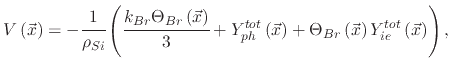
The corresponding balance equations can be written as
silicon etching.
The corresponding balance equations can be written as
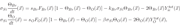 |
(202) |
 |
(203) |
This model uses bromine properties from [11] in order to generate the topography of the etched silicon profile
shown in Figure 5.8. The simulations use the following fluxes during the etching process:
![]() ,
,
![]() , and
, and
![]() .
.
The SiO![]() mask opening is set to 70nm while etching continued for 410s, as was performed in [86]. The simulation was performed
in order to analyze the effects on the etching process, when the silicon dioxide layer has tapered walls. As can be seen, when the SiO
mask opening is set to 70nm while etching continued for 410s, as was performed in [86]. The simulation was performed
in order to analyze the effects on the etching process, when the silicon dioxide layer has tapered walls. As can be seen, when the SiO![]() is angled at
89
is angled at
89
![]() , a relatively flat vertical sidewall is seen in the silicon. However, even a slight tapering, shown at 86
, a relatively flat vertical sidewall is seen in the silicon. However, even a slight tapering, shown at 86
![]() , results in
a silicon etched sidewall topography with an additional erosion width. These simulations confirm the experimental and simulated results from [86].
, results in
a silicon etched sidewall topography with an additional erosion width. These simulations confirm the experimental and simulated results from [86].
![\includegraphics[width=0.7\linewidth]{chapter_process_modeling/figures/SiEtching.eps}](img751.png)