Fig. 3.7 shows the band diagram and the electrostatic potential in
a metal-oxide-semiconductor structure for different voltages at the metal
contact [108,109,110]. A central quantity is the work
function which is defined as the energy required to extract an electron from
the FERMI energy to the vacuum level. The work function of the semiconductor
is
 |
(3.43) |
where  denotes the electron affinity of the semiconductor. The work
function difference between the work function in the metal
denotes the electron affinity of the semiconductor. The work
function difference between the work function in the metal

 and the work
function in the semiconductor
and the work
function in the semiconductor
 is
is
 |
(3.44) |
The values of
and
 depend on the material, as shown in
Table 3.1 [100,111,112]. However, the actual
value of the work function of a metal deposited on SiO
depend on the material, as shown in
Table 3.1 [100,111,112]. However, the actual
value of the work function of a metal deposited on SiO is not exactly the
same as that of the metal in vacuum [112].
is not exactly the
same as that of the metal in vacuum [112].
As long as BOLTZMANN statistics can be applied, the FERMI potential
 depends on the doping concentration of the semiconductor in the following way:
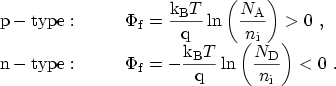 |
(3.45) |
The concentration-independent part of (3.44) is labeled
 :
:
 |
(3.46) |
The voltage which has to be applied to achieve flat bands is denoted the
flatband voltage. If we deviate from this voltage, a space charge region forms
near the interface between the dielectric and the semiconductor. The total
potential drop across this space charge region is the surface potential
 . Due to this potential all energy levels in the conduction and valence
bands are shifted by a constant amount, therefore
. Due to this potential all energy levels in the conduction and valence
bands are shifted by a constant amount, therefore
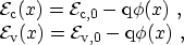 |
(3.47) |
where
 and
and
 are the conduction and valence bands in the
flatband case. Note that in the flatband case
are the conduction and valence bands in the
flatband case. Note that in the flatband case
 in the whole
structure.
in the whole
structure.
Figure 3.7:
Band diagram and electrostatic potential in an
nMOS structure (negative work function difference) in accumulation, under
flatband condition, without bias, and under inversion condition.
|
|
In metals the FERMI energy is located at a higher energy level than the
conduction band. The difference between the conduction band edge in the metal
and the FERMI energy in the metal can be calculated considering the
free-electron theory of metals which assumes that the metal electrons are
unaffected by their metallic ions. The sphere of radius
 (the FERMI
wave vector) contains all occupied levels and determines the electron
concentration
(the FERMI
wave vector) contains all occupied levels and determines the electron
concentration
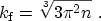 |
(3.48) |
The values of the metal work function and
for various metals are
summarized in the right part of Table 3.1 [114]. The value of
 can then directly be calculated from the carrier concentration
assuming a parabolic dispersion relation and a MAXWELLian distribution
function.
can then directly be calculated from the carrier concentration
assuming a parabolic dispersion relation and a MAXWELLian distribution
function.
At the semiconductor side the height of the energy barrier is given by
 for electrons and
 for holes. Note that in the derivation
of the TSU-ESAKI formula the barrier height
for holes. Note that in the derivation
of the TSU-ESAKI formula the barrier height
 , which denotes the
energetic difference between the FERMI energy and the band edge in the
dielectric, is used. Depending on the considered tunneling process,
must be calculated from
or
.
, which denotes the
energetic difference between the FERMI energy and the band edge in the
dielectric, is used. Depending on the considered tunneling process,
must be calculated from
or
.
A. Gehring: Simulation of Tunneling in Semiconductor Devices
![\includegraphics[width=.99\linewidth]{figures/mosBarrierBiasHTML}](img384.png)