3.4.2 Image Force Correction
When an electron approaches a dielectric layer, it induces a positive charge
on the interface which acts like an image charge within the layer. This
effect leads to a reduction of the barrier height for both electrons and
holes [115,116,117]: The conduction band bends
downward and the valence band bends upward, respectively. To account for this
effect, the band edge energies (3.47) must be modified
 |
(3.49) |
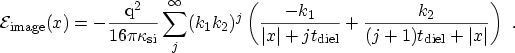
where the image force correction in the dielectric with thickness
 is calculated
as [118]
is calculated
as [118]
 |
(3.50) |
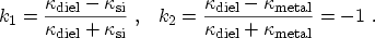
where  is at the interface to the dielectric. The symbols
  and
and  are calculated from the dielectric permittivities in the neighboring materials
 |
(3.51) |
Here, accounts for the interface between the insulator and the metal and
evaluates to  .
.
In the semiconductor the band edge energies are also altered
 |
(3.52) |
In practice it is sufficient to evaluate the sums in (3.50) and
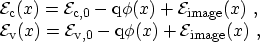
(3.52) up to  [119]. Fig. 3.8 shows the
band edge energies in an MOS structure for a dielectric layer with a thickness
of 2nm and different dielectric permittivities for an applied bias of 0V
(left) and 2V (right). A lower dielectric permittivity leads to a stronger
band bending due to the image force and therefore strongly influences the
transmission coefficient.
[119]. Fig. 3.8 shows the
band edge energies in an MOS structure for a dielectric layer with a thickness
of 2nm and different dielectric permittivities for an applied bias of 0V
(left) and 2V (right). A lower dielectric permittivity leads to a stronger
band bending due to the image force and therefore strongly influences the
transmission coefficient.
However, there is still some uncertainty if the image force has to be
considered for tunneling calculations. While it is used in some
works [120,121,122,119], others neglect it or report
only minor influence on the
results [123,124,125,126,127]. For rigorous
investigations, however, its necessary to include it in the simulations. This,
however, raises the need for a high spatial resolution along the
dielectric. Simple models like the analytical WKB formula or the GUNDLACH
formula are not valid for this case, as described in the following
sections. It may therefore be justified to account for the image force barrier
lowering by correction factors.
Figure 3.8:
Effect of the image force in an nMOS device with a
dielectric thickness of 2 nm at a gate bias of 0 V (left) and
2 V (right).
|
|
A. Gehring: Simulation of Tunneling in Semiconductor Devices
![\includegraphics[width=.49\linewidth]{figures/imageForceNobias}](img397.png)
![\includegraphics[width=.49\linewidth]{figures/imageForceBias}](img398.png)