3.2 Effect of Strain on Silicon Band Structure

3.2.1 Unstrained Silicon


SVG-Viewer needed.


Figure 3.2: The first Brillouin zone of the relaxed silicon lattice is shown. The valley positions and high symmetry points are shown as well.


PIC

Figure 3.3: The silicon band structure calculated by the pseudopotential method (CB is the conduction band, and VB is the valence band) is described. The VB edges are located exactly at the Γ-point and the minimum of the lowest CB lies on the symmetry Δ line close to the X-point. The lowest two CBs degenerate exactly at the X-point.


SVG-Viewer needed.


Figure 3.4: Left: constant energy surface of unstrained silicon (six-fold degeneracy) is shown, right: conduction band splitting under shear tensile strain on (001) plane is shown. The red (green) color-fill signifies high (low) electron concentration.


Directions

Coordinate

Remark


Γ

(0,0,0)

Center of the Brillouin zone (k space origin)

X

(0,0,1)

Middle of square faces

L

(12,-12,12)

Middle of hexagonal faces

K

(0,-3
4,3
4)

Middle of edge shared by two hexagons

U

(1
4,-1
4,1)

Middle of edge shared by a hexagons and a square

W

(0,-1
2,1)

Middle of edge shared by two hexagons and a square

Δ

Directed from Γ to X

Λ

Directed from Γ to L

Directed from Γ to K


Table 3.1: The symmetry points of the first Brillouin zone in silicon are listed according to Figure 3.2 are listed.

The first Brillouin zone is defined as the primitive cell in the reciprocal lattice. 
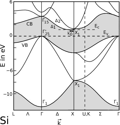
In silicon, the first Brillouin zone has a shape of a truncated octahedron (c.f. Figure 3.2), and is characterized by eight hexagonal faces and six square faces. The conduction band (CB) edge is located near the zone boundary X points along the Δ symmetry lines. The corresponding symmetry points and directions are tabulated in Table 3.1. The valence bands (VB) contain the last filled energy levels at T=0K, whereas the conduction bands are empty. The band gap Egap separates the CB from the VB. The band structure is usually visualized by plotting En(k) along symmetry lines.

The general band structure of unstrained silicon can be sketched as in Figure 3.3. The principal conduction band CB minima are located along the [100], [010], and [001] directions at a distance of about 85% from the Γ-point to the X-points (or equivalently, 15% from the X-point to the Γ-point). The energy of the two lowest CBs are degenerate at the X-points. Close to the CB edge, the band structure can be approximated by constant ellipsoidal energy surfaces (c.f. Figure 3.4 left) and a parabolic energy dispersion [140141]. The semi-axes of the ellipse show the direction of the longitudinal ml and the transversal electron mass mt. The six-fold degeneracy of the valleys arise due to the symmetry of the lattice along the [100], [010], and [001] directions. The electrons occupy all of these 3 pairs equally, making the transport isotropic.

3.2.2 Strained Silicon

The application of stress modifies the various symmetry properties, causes a change in the band structure, and thus modifies the effective mass which leads to the mobility enhancement [142]. Th values of ml and mt change under the influence of shear strain [140]. The shear strain also induces a shift in the energy levels of the conduction band and the valence band [72]. This energy shift can be calculated by using the deformation potential theory [72]. The six-fold degenerate Δ6 valleys in silicon are split into a two-fold degenerate Δ2 valley pair along [001] direction, and a four-fold degenerate Δ4 valley pair located along the other two axes. Strain results in lowering (increasing) energy of the Δ24) valley pair(s) [72143141]. Under this condition, the electron population of the Δ24) valley pair(s) is increased (decreased), c.f. Figure 3.4.