![\begin{figure}
\begin{center}
\resizebox{7.8cm}{!}{
\psfrag{a} {$\scriptstyle a)...
...ncludegraphics[width=7.8cm,angle=0]{figures/vi-rel.eps}}\end{center}\end{figure}](img37.gif) |
The independent variables of the NA are the node voltages ![]() of each
circuit node to a reference node which can be chosen arbitrarily. This choice
guarantees that KVL is fulfilled which requires that the sum of all
voltages around any loop in the circuit are zero. Considering an arbitrary
loop in an arbitrary circuit the sum of the voltages can be written as
of each
circuit node to a reference node which can be chosen arbitrarily. This choice
guarantees that KVL is fulfilled which requires that the sum of all
voltages around any loop in the circuit are zero. Considering an arbitrary
loop in an arbitrary circuit the sum of the voltages can be written as
| (2.1) |
Kirchhoff's current law (KCL) is applied to each node other than the reference node in the circuit such that the summation of the currents leaving the node is equal to zero. This procedure is best illustrated on the example circuit shown in Fig. 2.2. Summing the currents at all nodes one gets
| node 0 | : | G3 . ( |
= - J1 - J2 | (2.2) |
| node 1 | : | G1 . ( |
= J1 | (2.3) |
| node 2 | : | G2 . ( |
= J2 | (2.4) |
| node 3 | : | G1 . ( |
= 0 | (2.5) |
or in matrix and vector notation
![$ \underbrace{\left[ \begin{array}{cccc} G_{3} & & & -G_{3} \\ & G_{1} & & -G_{...
...} & G_{1} + G_{2} + G_{3} \end{array} \right] }_{\displaystyle \mathbb{Y}}^{}\,$](img48.gif) . . ![$ \underbrace{\left[ \begin{array}{c} \varphi_{0}\\ \varphi_{1}\\ \varphi_{2}\\ \varphi_{3}\\ \end{array} \right] }_{\displaystyle \boldsymbol{\varphi}}^{}\,$](img49.gif) =
= ![$ \underbrace{\left[ \begin{array}{c} - J_{1} - J_{2}\\ J_{1}\\ J_{2}\\ 0 \end{array} \right] }_{\displaystyle \mathbf{J}}^{}\,$](img50.gif) . . |
(2.6) |
The matrix
![]() is the admittance matrix of the circuit. However, it is
obvious that the equations (2.2) - (2.5) are not
independent. In general it can be shown that for a circuit containing N
nodes, exactly N - 1 independent KCL equations can be formulated
[72]. As the reference voltage is fixed anyway, there are N - 1
equations for the remaining N - 1 unknowns. The absolute value of the
reference voltage is of course arbitrary and normally assumed to be zero.
is the admittance matrix of the circuit. However, it is
obvious that the equations (2.2) - (2.5) are not
independent. In general it can be shown that for a circuit containing N
nodes, exactly N - 1 independent KCL equations can be formulated
[72]. As the reference voltage is fixed anyway, there are N - 1
equations for the remaining N - 1 unknowns. The absolute value of the
reference voltage is of course arbitrary and normally assumed to be zero.
Another important issue is that
![]() can be assembled by inspection on a
per-element basis. The admittance matrices of the devices can simply be
superpositioned to yield the circuit admittance matrix. Current sources
contribute to the current source vector
J. Therefore these
contributions are commonly refered to as stamps as they can be directly
stamped into the system matrix element per element without the need to
consider the rest of the circuit.
can be assembled by inspection on a
per-element basis. The admittance matrices of the devices can simply be
superpositioned to yield the circuit admittance matrix. Current sources
contribute to the current source vector
J. Therefore these
contributions are commonly refered to as stamps as they can be directly
stamped into the system matrix element per element without the need to
consider the rest of the circuit.
The admittance matrix for a conductance G reads

|
(2.7) |
JJ = 
|
(2.8) |
| yx, y |
|
|
J |
| n1 | G | - G | J0 |
| n2 | - G | G | - J0 |
Non-linear branch relations are handled by introducing linearized companion models. A general non-linear device with branch relation
| I = I( |
(2.9) |
| I( |
= 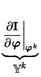 . . 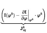 |
(2.10) |
| Jeqk | = I( |
(2.11) |
| ID | = 
|
(2.12) |
|
with
| ||
| ID | = IS . |
(2.13) |
| yx, y |
|
|
J |
| n1 | gmk | - gmk | Jeqk |
| n2 | - gmk | gmk | - Jeqk |
| gmk | =  |
(2.14) |
| Jeqk | = IDk - gm . VDk | (2.15) |
For circuits containing only conductances and current sources, the condition of the resulting equation system is very good. In this case the NA produces diagonal-dominant matrices which are well suited for iterative solution procedures. Two additional devices can be modeled using the NA, namely a voltage controlled current source (cf. Section 2.3.3.8) and the gyrator (cf. Section 2.3.3.12). These devices destroy the diagonal dominance of the circuit admittance matrix.
One disadvantage of the NA is the inadequate treatment of voltage sources. Ideal voltage sources and current controlled elements cannot be modeled with this approach. However, a very large class of integrated circuits can be accommodated by adding a provision for grounded sources. Other workarounds for floating voltage sources have been proposed which can be quite awkward to handle [53,65]. To model current dependencies small or negative resistances have been introduced which result in numerical instabilities [65].
![\begin{figure}
\begin{center}
\resizebox{7.8cm}{!}{
\psfrag{J1}{$\scriptstyle J_...
...ncludegraphics[width=7.8cm,angle=0]{figures/na-exa.eps}}\end{center}\end{figure}](img38.gif)