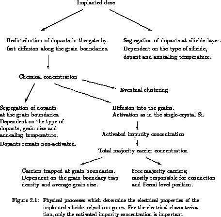
The activated impurity concentration close to the gate/oxide interface depends on two processes: the redistribution of the impurities and their activation.
There are two effects which affect the
 in the polysilicon gates:
 -
-  ) is much larger
than the junctions depth
( -
) is much larger
than the junctions depth
( -  ) [512][28].
Note that by decreasing the polysilicon-layer
thickness the chemical concentration in the gate increases [512]
as expected (assuming that no segregative silicide layer is presented).
) [512][28].
Note that by decreasing the polysilicon-layer
thickness the chemical concentration in the gate increases [512]
as expected (assuming that no segregative silicide layer is presented).
 is reported in [346] (by
 rapid thermal annealing (RTA) at
 C) and into CoSi
as well.
Contrary, a significant segregation of As into TiSi
at
C) and into CoSi
as well.
Contrary, a significant segregation of As into TiSi
at  C and
C and  C anneal is demonstrated in [28]. For
P a low segregation into WSi is obtained in [345] (by RTA
at C). No segregation of As into NiSi is observed (at
C anneal is demonstrated in [28]. For
P a low segregation into WSi is obtained in [345] (by RTA
at C). No segregation of As into NiSi is observed (at
 C 30s RTA) in [320].
polysilicon gates is reported in [412][300]. B
was uniformly distributed in the polysilicon. The B concentration was
limited to
C 30s RTA) in [320].
polysilicon gates is reported in [412][300]. B
was uniformly distributed in the polysilicon. The B concentration was
limited to  (assuming sufficiently high doses)
for C annealing temperature. The rest of B segregates into
TaSi layer which has a much larger solubility limit. Note that by
decreasing the annealing temperature (under C) a higher
saturation concentration of B could be achieved due to less segregation
into TaSi, thus improving the gates.
Decreasing the temperature also reduces risk of B-penetration through the
thin oxide. A significant B segregation into WSi
(assuming sufficiently high doses)
for C annealing temperature. The rest of B segregates into
TaSi layer which has a much larger solubility limit. Note that by
decreasing the annealing temperature (under C) a higher
saturation concentration of B could be achieved due to less segregation
into TaSi, thus improving the gates.
Decreasing the temperature also reduces risk of B-penetration through the
thin oxide. A significant B segregation into WSi is found for
C anneal in [188], as well. However, after
is found for
C anneal in [188], as well. However, after  RTA at
 C the chemical concentration of B is increased to
 . Similarly, after RTA at C a
chemical concentration of B in the polysilicon as large as
. Similarly, after RTA at C a
chemical concentration of B in the polysilicon as large as
 is achieved for the WSi silicide
in [346][345]. No segregation of B into NiSi is observed
(at C
is achieved for the WSi silicide
in [346][345]. No segregation of B into NiSi is observed
(at C  RTA) [320].
in [371][369], for WSi in [188][81], for
TaSi in [363], for TiSi in [276][81] and for
NiSi in [320]. Compact model of the dopant diffusion in
silicides is presented in [81]. Note that the interdiffusion can
be completely avoided for NiSi, due to a very low temperature needed for
silicidation (C).
RTA) [320].
in [371][369], for WSi in [188][81], for
TaSi in [363], for TiSi in [276][81] and for
NiSi in [320]. Compact model of the dopant diffusion in
silicides is presented in [81]. Note that the interdiffusion can
be completely avoided for NiSi, due to a very low temperature needed for
silicidation (C).
The  of dopants depends on the location of
impurity atoms. It is believed that atoms which segregate at grain boundaries
remain there non-activated, while the atoms which diffuse into the grains are
activated there as in single-crystal silicon, after annealing.
of dopants depends on the location of
impurity atoms. It is believed that atoms which segregate at grain boundaries
remain there non-activated, while the atoms which diffuse into the grains are
activated there as in single-crystal silicon, after annealing.
Experiments have shown that As and P segregate significantly at the grain
boundaries [289]. Decreasing the annealing temperature the segregation
becomes enhanced and more atoms remain non-activated in the polysilicon and
vice versa. These processes
repeat by cycling the annealing temperature. A simple and, for engineers,
useful model for the activated impurity concentration in the polysilicon in
the steady-state as a function of the chemical impurity concentration, type of
impurity, average grain size and annealing temperature has been developed
in [289] (see also [403][28]). An activation which lies in
the interval from few percent [449] to
 is typically reported in literature. As a consequence, the activated impurity
concentration in the As and P implanted gates can be very low. By applying RTA
the activation of P and As in the polysilicon gates can be significantly
improved due to high temperature, while keeping the source/drain junctions
unaltered during this short time. An enlarged activation of As by increasing
annealing temperature and/or employing RTA is demonstrated
in [512][449][281].
is typically reported in literature. As a consequence, the activated impurity
concentration in the As and P implanted gates can be very low. By applying RTA
the activation of P and As in the polysilicon gates can be significantly
improved due to high temperature, while keeping the source/drain junctions
unaltered during this short time. An enlarged activation of As by increasing
annealing temperature and/or employing RTA is demonstrated
in [512][449][281].
There is no segregation of B at the grain boundaries in the polysilicon, as
determined for the annealing temperature between  C and
C and  C and
chemical concentration of
C and
chemical concentration of  in [289], in other
words, the activation of B is complete.
in [289], in other
words, the activation of B is complete.
At the end of this introductory section a short comment will be made on the
 . It consists of the penetration
of B from the doped gate through the thin gate-oxide into the bulk of MOS
devices during the high-temperature anneal. B atoms are activated in the bulk
and form a shallow acceptor-type layer close to the oxide interface. This
effect is usually manifested as a large positive shift in flat-band and
threshold voltage after the gate anneal, similarly as for the gate depletion.
The voltage shift due to boron penetration can be in the same direction as the
shift due to gate depletion or the opposite. Both effects, boron penetration
and gate depletion are strongly related to thin oxides and gate processing.
B-penetration strongly increases when the annealing temperature exceeds some
limit [497][450]. The presence of hydrogen in the annealing ambient
enhances the effect [450]. Similarly, it is found that the presence of
fluorine significantly increases the B-penetration [454][368][22].
Note that a controlled incorporation of fluorine can be used to improve the
gate-oxide hardness on hot-carriers. A combined effect of fluorine and hydrogen
on the enhanced B-penetration is discussed in [454]. A detailed
modeling of B-penetration using process and device simulation is presented
in [370][368]. B-penetration will not be considered in this study.
. It consists of the penetration
of B from the doped gate through the thin gate-oxide into the bulk of MOS
devices during the high-temperature anneal. B atoms are activated in the bulk
and form a shallow acceptor-type layer close to the oxide interface. This
effect is usually manifested as a large positive shift in flat-band and
threshold voltage after the gate anneal, similarly as for the gate depletion.
The voltage shift due to boron penetration can be in the same direction as the
shift due to gate depletion or the opposite. Both effects, boron penetration
and gate depletion are strongly related to thin oxides and gate processing.
B-penetration strongly increases when the annealing temperature exceeds some
limit [497][450]. The presence of hydrogen in the annealing ambient
enhances the effect [450]. Similarly, it is found that the presence of
fluorine significantly increases the B-penetration [454][368][22].
Note that a controlled incorporation of fluorine can be used to improve the
gate-oxide hardness on hot-carriers. A combined effect of fluorine and hydrogen
on the enhanced B-penetration is discussed in [454]. A detailed
modeling of B-penetration using process and device simulation is presented
in [370][368]. B-penetration will not be considered in this study.