As mentioned at the beginning, the single-crystal band model will be assumed for
the polysilicon gate in this section. In other words we did not account for
the grain-structure of polysilicon. The validity of such an approach depends on
the ratio between the activated dopant concentration in the gate  and the
equivalent volume trap density in the polysilicon
and the
equivalent volume trap density in the polysilicon  . The
densities near the gate/oxide interface are particularly important.
is given by the quotient of the surface-trap density at grain
boundaries
. The
densities near the gate/oxide interface are particularly important.
is given by the quotient of the surface-trap density at grain
boundaries  and the average grain size
  [422]. Two
conditions can occur:
[422]. Two
conditions can occur:
 holds, the charge trapped at the grain
boundaries is much smaller than the free charge of the majority carriers
within the grains. Even if the grains are depleted in some part of the
gate due to the terminal bias, the space charge descending from the
doping is dominant over the space charge coming from an eventual trapped
charge. The trapped charge has minor impact on the neutral Fermi level
and an average space charge density. Therefore, it may be omitted from the
Poisson equation in a first approximation. Note that this is not the case
for the transport problem in polysilicon - low barriers at the grain
boundaries also affect the current if
holds [516][298][247][235]. We consider, however, a pure
electrostatic problem in this study.
is comparable to or less than the trap-effect
is dominant and dictates all electrical properties of the polysilicon. The
Fermi level position, potential drop in the gate and especially, the gate
capacitance become sensitive functions of the model parameters such as
density of the traps at grain boundaries, their energy distribution
and the average grain size.
holds, the charge trapped at the grain
boundaries is much smaller than the free charge of the majority carriers
within the grains. Even if the grains are depleted in some part of the
gate due to the terminal bias, the space charge descending from the
doping is dominant over the space charge coming from an eventual trapped
charge. The trapped charge has minor impact on the neutral Fermi level
and an average space charge density. Therefore, it may be omitted from the
Poisson equation in a first approximation. Note that this is not the case
for the transport problem in polysilicon - low barriers at the grain
boundaries also affect the current if
holds [516][298][247][235]. We consider, however, a pure
electrostatic problem in this study.
is comparable to or less than the trap-effect
is dominant and dictates all electrical properties of the polysilicon. The
Fermi level position, potential drop in the gate and especially, the gate
capacitance become sensitive functions of the model parameters such as
density of the traps at grain boundaries, their energy distribution
and the average grain size.
 have been experimentally
estimated for small grain polysilicon in [403][366][289] and in
studies cited in these references. Assuming e.g.
have been experimentally
estimated for small grain polysilicon in [403][366][289] and in
studies cited in these references. Assuming e.g.  it follows
  . For larger grain,
becomes smaller. If we restrict ourselves to the active dopant
concentrations
. For larger grain,
becomes smaller. If we restrict ourselves to the active dopant
concentrations  the error due to the trap-effect
seems to be reasonably small. Note that the traps become important in lightly
doped gates, like those in [367]. In fact, we have no interest to
accurately model low doped gates, employing physical models with many hardly
available parameters, since these gates exhibit a too large depletion effect
for an application in device design. The effect of traps at grain boundaries
will also be addressed in Section 2.3.
the error due to the trap-effect
seems to be reasonably small. Note that the traps become important in lightly
doped gates, like those in [367]. In fact, we have no interest to
accurately model low doped gates, employing physical models with many hardly
available parameters, since these gates exhibit a too large depletion effect
for an application in device design. The effect of traps at grain boundaries
will also be addressed in Section 2.3.
The rigid-parabolic-band model is assumed to be valid in the gate for dopant
concentrations of interest  [296][295][294][292]. The rigid-band model means that the
dispersion relation
[296][295][294][292]. The rigid-band model means that the
dispersion relation  does not change with respect to pure
silicon, but only shifts on the energy scale due to the heavy-doping effects.
As a consequence, the effective densities of states for the conduction and
valence band (
does not change with respect to pure
silicon, but only shifts on the energy scale due to the heavy-doping effects.
As a consequence, the effective densities of states for the conduction and
valence band ( and
and  , respectively) are invariant of spatial
coordinates. In this concept we account for the states in the band
tails [239] by
additionally increasing the rigid shift of the conduction and valence band
caused by the many-body effects [267]. The rigid-parabolic-band model
is not only simple and convenient for analytical and numerical handling, but
also supported by experiments: assuming the bands in heavily doped silicon
to be parabolic close to band edges, but only shifted in the energy level, the
experimental data of differential tunneling conductance [2] and
radiative recombination [110], both at very low temperature
(
, respectively) are invariant of spatial
coordinates. In this concept we account for the states in the band
tails [239] by
additionally increasing the rigid shift of the conduction and valence band
caused by the many-body effects [267]. The rigid-parabolic-band model
is not only simple and convenient for analytical and numerical handling, but
also supported by experiments: assuming the bands in heavily doped silicon
to be parabolic close to band edges, but only shifted in the energy level, the
experimental data of differential tunneling conductance [2] and
radiative recombination [110], both at very low temperature
( and
and  ), have been successfully explained. It is commonly accepted
that the rigid-parabolic-band model is a reasonable approach to describe the
carrier transport in heavily doped quasi-neutral regions [358]. The
same approach is often employed to model the current and the recombination of
minority carriers injected into heavily doped quasi-neutral
emitter [327][307][190][94] and base [470][438] of
bipolar transistors. However, regarding modeling heavily doped
space-charge regions, there are likely to be strong limitations to this
approach, because of appearing deep band-tails due to lack of
screening [280][61]. A detailed discussion of this topic is given in
Section 2.3 after demonstrating that the
rigid-parabolic-band approach fails to fit accurately the experimental
), have been successfully explained. It is commonly accepted
that the rigid-parabolic-band model is a reasonable approach to describe the
carrier transport in heavily doped quasi-neutral regions [358]. The
same approach is often employed to model the current and the recombination of
minority carriers injected into heavily doped quasi-neutral
emitter [327][307][190][94] and base [470][438] of
bipolar transistors. However, regarding modeling heavily doped
space-charge regions, there are likely to be strong limitations to this
approach, because of appearing deep band-tails due to lack of
screening [280][61]. A detailed discussion of this topic is given in
Section 2.3 after demonstrating that the
rigid-parabolic-band approach fails to fit accurately the experimental  -
- data of devices with moderately doped gates.
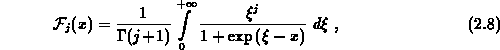
In the rigid-parabolic-band model the carrier concentrations in the gate can be simply written
with  the Fermi integral of order
  . In this work
Fermi integrals are defined in the normalized form
. In this work
Fermi integrals are defined in the normalized form
with  being the Gamma function. The band edges in the gate are
given by
being the Gamma function. The band edges in the gate are
given by
The spatial variations of the band edges in the ideal silicon band
 and
and  are due to inhomogeneity in the dopant
concentration and the electric-field penetration into the gate. The band
edges
are due to inhomogeneity in the dopant
concentration and the electric-field penetration into the gate. The band
edges  and
and  vary in addition because of spatially variable
band-gap narrowing
vary in addition because of spatially variable
band-gap narrowing  and
and  which represents the
shift of conduction band downward and the valence band upward, as introduced
in [358]. Let the potential
which represents the
shift of conduction band downward and the valence band upward, as introduced
in [358]. Let the potential  in the gate be defined as the
potential difference between the intrinsic Fermi level in the ideal silicon
band
in the gate be defined as the
potential difference between the intrinsic Fermi level in the ideal silicon
band  and the reference Fermi level in the source of MOS device.
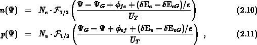
The carrier concentrations in the gate become
and the reference Fermi level in the source of MOS device.
The carrier concentrations in the gate become
with the potential at the gate-contact
representing the boundary condition. From the neutral carrier concentration at the gate-contact it follows
The neutral electron concentration  equals to the activated impurity
concentration
equals to the activated impurity
concentration  at the gate-contact in
  -type gate. For
  -type of
gate,
-type of
gate,  holds.
  in 2.13
is the inverse Fermi integral. With
in 2.13
is the inverse Fermi integral. With  or
or  calculated
by 2.13, the second quantity follows from
calculated
by 2.13, the second quantity follows from
where  is the ideal silicon band gap
and
is the ideal silicon band gap
and  denotes the total
band-gap narrowing at the gate-contact. The Fermi barrier in the gate
occurring in the voltage conversation 2.6 may be related to
with
denotes the total
band-gap narrowing at the gate-contact. The Fermi barrier in the gate
occurring in the voltage conversation 2.6 may be related to
with
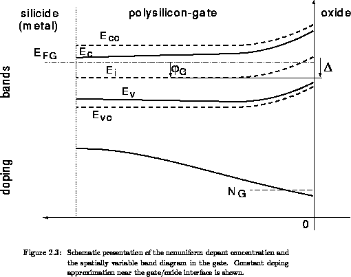
It holds that  , as is evident from
Figure 2.3.
, as is evident from
Figure 2.3.
Previous relationships account properly for a position-dependent band-gap
narrowing in the gate. They are implemented in a two-dimensional numerical
model of MOSFETs, as introduced in Section 2.4. To
simplify the expressions for analytical modeling we adopt a constant doping
approximation in the gate near the gate/oxide interface as schematically shown
in Figure 2.3. The necessary width of this uniform region
with concentration is only a few extrinsic Debye length
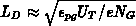 wide. For a minimal
 the maximal width of about
 may be estimated, which is much shorter than
the polysilicon thickness. The remaining part of the gate is in quasi-neutral
condition because of heavy doping and the impurity profile in this region is not
important for our study
may be estimated, which is much shorter than
the polysilicon thickness. The remaining part of the gate is in quasi-neutral
condition because of heavy doping and the impurity profile in this region is not
important for our study .
Consequently, the quantity
.
Consequently, the quantity  does not vary from the
gate-contact until the region close to the gate/oxide interface where the
potential begins to change due to electric-field penetration. Thereby, both,
does not vary from the
gate-contact until the region close to the gate/oxide interface where the
potential begins to change due to electric-field penetration. Thereby, both,
 and
and  may be determined with respect to the uniform
concentration .
may be determined with respect to the uniform
concentration .
The surface potential is obtained after integration of the Poisson
equation in the homogeneous part of the gate, using the conditions
 and
and  for
for  and
and
 and
and  at
at  . Practically, the
field decreases from
. Practically, the
field decreases from  to a negligible value after a few
  from the
gate/oxide interface. Employing the well known integration technique shown in
Appendix A the relationship between the surface field and
the surface potential follows
from the
gate/oxide interface. Employing the well known integration technique shown in
Appendix A the relationship between the surface field and
the surface potential follows
Note that and vanish due to the constant
doping assumed.  in 2.16 is the
Fermi integral of order
in 2.16 is the
Fermi integral of order  . Consistent with Figure 2.2 and
the definition of , it follows
. Consistent with Figure 2.2 and
the definition of , it follows  for
for  , while
 holds for
  . At the flat-band in the gate
 and
and  . The three terms at the left-hand-side
in 2.16 model accumulation, depletion and inversion in the
-polysilicon gate, respectively.
. The three terms at the left-hand-side
in 2.16 model accumulation, depletion and inversion in the
-polysilicon gate, respectively.