With the drain-source bias expression 2.6 for
the voltage conversation still holds. The spatially variable surface potential
becomes  , where
  is the potential
difference between the quasi-Fermi level for electrons in the channel and
Fermi level in the source due to drain-source bias.
is the potential
difference between the quasi-Fermi level for electrons in the channel and
Fermi level in the source due to drain-source bias.  denotes the
relative surface potential with respect to the level laying
denotes the
relative surface potential with respect to the level laying  above
the quasi-Fermi level for electrons in inversion layer. The inversion-layer
charge
above
the quasi-Fermi level for electrons in inversion layer. The inversion-layer
charge  is given by 2.20 which is generally valid,
with
is given by 2.20 which is generally valid,
with  and
and  determined by the
system 2.4, 2.6 and the
determined by the
system 2.4, 2.6 and the  relation for bulk. To remove the voltage drop
  from the system of
equations an explicit expression
from the system of
equations an explicit expression  is necessary. This
relation follows from equations 2.2, 2.4
and 2.6 which are valid in the presence of a nonzero
is necessary. This
relation follows from equations 2.2, 2.4
and 2.6 which are valid in the presence of a nonzero
 too. Assuming the gate to be in depletion it follows
 . Depletion in the gate is typical for
both,
. Depletion in the gate is typical for
both,  -gate/-channel and
  -gate/-channel devices biased regularly.
A simple substitution of variables leads to a square equation with respect to
. Applying the condition
-gate/-channel devices biased regularly.
A simple substitution of variables leads to a square equation with respect to
. Applying the condition  one obtains the physical solution
with  being some corrected gate voltage given by
In the absence of a significant interface and oxide charge, for a vanishing
and when the oxide/bulk interface is inverted, it follows
 . Remember that
  is a bias applied on the
terminals. From 2.30 the reduction of gate bias due to gate
depletion becomes
is a bias applied on the
terminals. From 2.30 the reduction of gate bias due to gate
depletion becomes
When , given by 2.30, is replaced in the voltage
conversation relationship 2.6, the obtained system of equations
only contains and as position-variable quantities. This
system may be applied to derive an analytical MOSFET model in an analogous way
as for equipotential gate MOSFETs
(e.g. [204][164][84][41]). For example, assuming
constant mobility and  in strong inversion, an
expression of the form
in strong inversion, an
expression of the form  may be simply derived
in the triode region.
may be simply derived
in the triode region.  is the current without gate depletion and
 given in form of a serial expansion represents the
reduction of current due to gate depletion.
given in form of a serial expansion represents the
reduction of current due to gate depletion.
We may judge  to be the figure of merit of ``gate-drive'' in MOSFETs, since
the charge
to be the figure of merit of ``gate-drive'' in MOSFETs, since
the charge  is determined primarily by in strong inversion. Suppose
that the gate bias induces the surface field
is determined primarily by in strong inversion. Suppose
that the gate bias induces the surface field  and the surface
potential
and the surface
potential  in a device with equipotential gate. The same gate
bias induces surface field
in a device with equipotential gate. The same gate
bias induces surface field  , the relative potential
  and
the potential drop in the gate in the same device, but with a
nondegenerate gate. The degradation of the gate-drive may be defined by
and
the potential drop in the gate in the same device, but with a
nondegenerate gate. The degradation of the gate-drive may be defined by
 . For zero drain-source bias (
 ), it follows
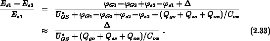
The terms  and
and  are small and even cancel each other, allowing the approximation on the
right-hand-side in 2.33. If the total interface and oxide
charge is negligible, the degradation-criterion 2.33 is
equivalent to 2.32.
are small and even cancel each other, allowing the approximation on the
right-hand-side in 2.33. If the total interface and oxide
charge is negligible, the degradation-criterion 2.33 is
equivalent to 2.32.
The characteristic ratio
determines the reduction of the gate bias. Note that the gate-depletion effect
is dependent on the type of gate-insulator (permittivity  ) and
the square of the oxide thickness, but only linearly on the gate doping and
applied bias
) and
the square of the oxide thickness, but only linearly on the gate doping and
applied bias  . The effect is independent of temperature.
Applying different scaling rules on
. The effect is independent of temperature.
Applying different scaling rules on  and the supply voltage ,
the gate-depletion effect becomes more or less severe by miniaturization. For
example, assuming
and the supply voltage ,
the gate-depletion effect becomes more or less severe by miniaturization. For
example, assuming 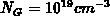
 for a device with
  and
and  the
corresponding reduction is calculated to be
the
corresponding reduction is calculated to be  at
at
 , while
for the device in Figure 2.18 with
, while
for the device in Figure 2.18 with  and
and  the reduction of drain current is
  at
at
 .
.
Note that the recent development shows a tendency to reduce the oxide thickness
under the  limit, but to keep the supply voltage high in designing CMOS
technology of deep-submicrometer level. Some examples represent a
limit, but to keep the supply voltage high in designing CMOS
technology of deep-submicrometer level. Some examples represent a
 subquarter-
 CMOS technology with the proposed
  supply [351]; with
  gate-length
-channel MOSFET in [472];
gate-length
-channel MOSFET in [472];  with
gate-length -channel MOSFET in [393] and
with
gate-length -channel MOSFET in [393] and  with
CMOS technology in [476]. These data should be compared
with -oxide thickness quarter- devices with only
with
CMOS technology in [476]. These data should be compared
with -oxide thickness quarter- devices with only  supply
discussed in earlier studies [20].
supply
discussed in earlier studies [20].
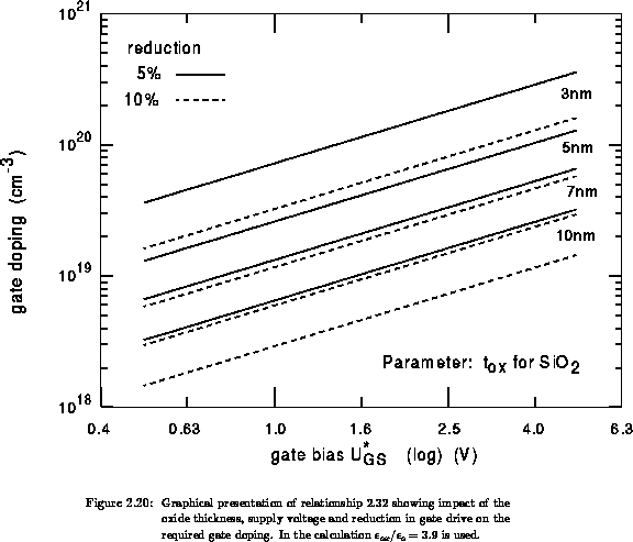
Figure 2.20 displays relationship 2.32
in a convenient engineering way. The ordinate shows the activated impurity
concentration near the gate/oxide interface  necessary to suppress the
gate depletion under the given degradation level (
necessary to suppress the
gate depletion under the given degradation level ( and
and  ) at specific
supply voltage (abscise). Parameters are the oxide thickness for SiO
) at specific
supply voltage (abscise). Parameters are the oxide thickness for SiO and
relative bias reduction
and
relative bias reduction  . Evidently, for very thin
oxides (
. Evidently, for very thin
oxides ( ) a quite high is necessary to suppress the degradation.
An important fact to note is that these are higher than those often
found in
) a quite high is necessary to suppress the degradation.
An important fact to note is that these are higher than those often
found in  dual-gate CMOS technology today [512][412][188].
The dependence of the gate-depletion effect on the square of the oxide
thickness could be important with regard to possible applications of gate
insulators with very high permittivity. Some examples are TaO with
with
 , [342][341][322]
and Ba
, [342][341][322]
and Ba Sr
Sr TiO
TiO with
with  up to
up to
 [138]. Such insulators have become demanding in design of
64Mb, 256Mb and beyond DRAM's [427][122]. The author is not
aware of attempts to fabricate MOSFETs with a high-permittivity gate-insulator
or with some layer in the gate insulator from those materials. Apart from
technological and reliability problems involved at fabrication and
operation of such MOSFETs, they would exhibit higher transconductances and
drain currents than are even possible with SiO gate-dielectric. Since the
equivalent insulator thickness is reduced by factor
[138]. Such insulators have become demanding in design of
64Mb, 256Mb and beyond DRAM's [427][122]. The author is not
aware of attempts to fabricate MOSFETs with a high-permittivity gate-insulator
or with some layer in the gate insulator from those materials. Apart from
technological and reliability problems involved at fabrication and
operation of such MOSFETs, they would exhibit higher transconductances and
drain currents than are even possible with SiO gate-dielectric. Since the
equivalent insulator thickness is reduced by factor
 , the gate capacitance
  becomes
 times higher than that of SiO-film with the
same thickness. In a simple estimation the maximum in the channel is
determined by
times higher than that of SiO-film with the
same thickness. In a simple estimation the maximum in the channel is
determined by  , where
  is the
maximal field strength allowed in the oxide. For TaO we estimate
is the
maximal field strength allowed in the oxide. For TaO we estimate
 , where
 is the breakdown field [340][322].
However, a high which induces a large , results in a high
is the breakdown field [340][322].
However, a high which induces a large , results in a high  and an increased lost in the gate drive due to gate depletion ( curve in
Figure 2.20 and beyond are interesting here). The gate
materials other than doped polysilicon would be probably required in such
devices.
and an increased lost in the gate drive due to gate depletion ( curve in
Figure 2.20 and beyond are interesting here). The gate
materials other than doped polysilicon would be probably required in such
devices.