The semiconductor capacitance in the gate may be defined by
where 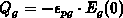 is the total charge in the gate per unit
area. Here, as throughout the whole appendix, we omit the interface and bulk
traps in consideration. In order to find
is the total charge in the gate per unit
area. Here, as throughout the whole appendix, we omit the interface and bulk
traps in consideration. In order to find  , we
derived A.11 with respect to
, we
derived A.11 with respect to  . The expression for
  becomes
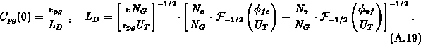
which is valid if  . For
. For  the flat-band condition
occurs in the gate and
the flat-band condition
occurs in the gate and  holds too, since the doping is assumed to be
uniform. Applying
holds too, since the doping is assumed to be
uniform. Applying  on the left and the right-hand-side
of A.18, after transformations, it leads the flat-band capacitance
on the left and the right-hand-side
of A.18, after transformations, it leads the flat-band capacitance
In deriving, we benefitted from A.12. In e.g.  -type of
silicon, the second summand due to holes in the expression for
-type of
silicon, the second summand due to holes in the expression for  is
negligible and reduces to formula 2.1. For MB
statistics we simply approximate
is
negligible and reduces to formula 2.1. For MB
statistics we simply approximate 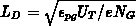 .
.
Adopting MB statistics for both carriers, relationship A.18 simplifies to