The electrical field and carrier distribution in the semiconductor bulk near the gate corner due to the gate/drain electrical-field fringing are analyzed in this appendix. The problem has been treated in a simplified manner in [356][355], including the effect of the lateral current flow. We employed a rigorous analytical approach to tackle this problem, but without accounting for the lateral current flow. The latter assumption is, however, valid in the charge pumping conditions we are interested in.
An analytical model is developed starting from several simplifying assumptions. The final evaluation of the analytical model, including the comparison with the numerical calculation, will show that a two-dimensional numerical model is indispensible to accurately describe the gate-corner/LDD-region fringing effect.
The problem with the coordinate system valid through this Appendix is shown
in Figure E.1 and E.2. The drain-sided gate edge
is the origin of the  -axis. In order to model the field distribution by an
analytical approach we introduce several assumptions:
-axis. In order to model the field distribution by an
analytical approach we introduce several assumptions:
 . There
is no lateral voltage drop from the heavy-doped region near the
drain contact to the gate/LDD subdiffusion region.
. There
is no lateral voltage drop from the heavy-doped region near the
drain contact to the gate/LDD subdiffusion region.
 . No depletion
of the gate area occurs.
. No depletion
of the gate area occurs.
 is the solution of the Laplace equation in the rectangular area presented in
Figure E.1, with
is the solution of the Laplace equation in the rectangular area presented in
Figure E.1, with  and
and  being the boundary conditions
between the oxide and the equipotential gate and semiconductor. We abbreviated
being the boundary conditions
between the oxide and the equipotential gate and semiconductor. We abbreviated
 .
.
The problem is solved by conformal transformations. Employing Schwarz-Christoffel's transformation on the dot-dashed contour presented in Figure E.1 we get
with  , where
  and
and  are constants determined below.
Transformation E.1 reduces the pristine problem to the Laplace
problem between two equipotential half-planes
are constants determined below.
Transformation E.1 reduces the pristine problem to the Laplace
problem between two equipotential half-planes  and
and
 at different potentials. To solve the latter problem we employ
a further transformation
at different potentials. To solve the latter problem we employ
a further transformation  , where
  is a constant. The final
problem is to obtain the field and the potential distribution between
two parallel infinitely long metallic plates at different potentials, which is
a trivial task. We assume
is a constant. The final
problem is to obtain the field and the potential distribution between
two parallel infinitely long metallic plates at different potentials, which is
a trivial task. We assume  , with
  being the potential we
are looking for. The equipotential lines are equidistant, given by
being the potential we
are looking for. The equipotential lines are equidistant, given by
 . From the boundary condition it follows that
  . The
electric field strength in the pristine region shown in
Figure E.2 is given by
. The
electric field strength in the pristine region shown in
Figure E.2 is given by  . Applying
the condition
. Applying
the condition  , we get
 . Considering the conditions at
  and
and  , as
well as
, as
well as  and
and  , it follows
  . Finally, the
potential distribution is determined by an implicit equation
. Finally, the
potential distribution is determined by an implicit equation
and the electric field strength by
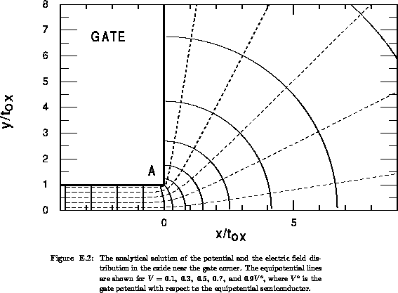
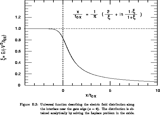
Figure E.2 shows the family of the equipotential curves and
the electric field-lines determined by relationships E.2
and E.3. For our analysis, the field distribution along the
-axis is particularly interesting. Assuming  and
in E.2 and E.3, the following relationship is obtained
and
in E.2 and E.3, the following relationship is obtained
where  is the perpendicular field in the oxide away from the
gate edge. Function E.4 describes the fall-off of the surface
electric field due to fringing when moving along the oxide/bulk interface from
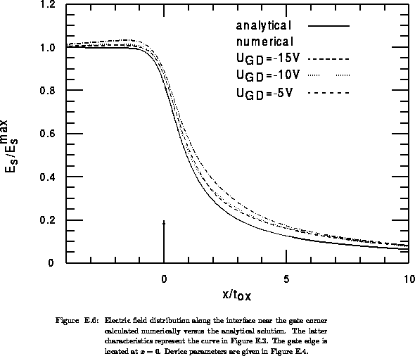
the gate edge towards the drain. This universal function is plotted in
Figure E.3. Under the gate electrode, the corner effect can be
neglected for distances larger than
is the perpendicular field in the oxide away from the
gate edge. Function E.4 describes the fall-off of the surface
electric field due to fringing when moving along the oxide/bulk interface from
the gate edge towards the drain. This universal function is plotted in
Figure E.3. Under the gate electrode, the corner effect can be
neglected for distances larger than  from the gate edge. At the other
side, toward the drain, due to fringing the field does not vanish very far from
the gate edge. A distance longer than
from the gate edge. At the other
side, toward the drain, due to fringing the field does not vanish very far from
the gate edge. A distance longer than  is necessary in order for
the transversal field to be judged as negligible. Note that our analysis is
valid if the gate height is much larger than the oxide thickness, as assumed at
the beginning.
is necessary in order for
the transversal field to be judged as negligible. Note that our analysis is
valid if the gate height is much larger than the oxide thickness, as assumed at
the beginning.
After obtaining the electric field along the oxide/semiconductor interface
for the applied bias  , we focus on the semiconductor region.
It has already been assumed that the transversal field in the silicon-dioxide
, we focus on the semiconductor region.
It has already been assumed that the transversal field in the silicon-dioxide
 is much larger than the lateral field at the interface. We further
adopt a more restrictive assumption that the transversal field component in the
silicon
is much larger than the lateral field at the interface. We further
adopt a more restrictive assumption that the transversal field component in the
silicon  can also be considered as
much larger than the lateral component. The Poisson equation in the
semiconductor reduces to one-dimensional form, giving the relationship between
can also be considered as
much larger than the lateral component. The Poisson equation in the
semiconductor reduces to one-dimensional form, giving the relationship between
 and the surface potential
with  . Formula E.5 is
derived for a uniformly doped semiconductor of
. Formula E.5 is
derived for a uniformly doped semiconductor of  -type.
Equation E.5 enables one to calculate the potential distribution
along the interface near the gate edge from the known field distribution.
Since the
-type.
Equation E.5 enables one to calculate the potential distribution
along the interface near the gate edge from the known field distribution.
Since the  -axis is directed from the semiconductor towards the interface,
negative imply positive and vice-versa. The surface carrier
concentrations are given with the well-known relationships
-axis is directed from the semiconductor towards the interface,
negative imply positive and vice-versa. The surface carrier
concentrations are given with the well-known relationships
 is the Fermi-barrier:
  . The
charge induced in the semiconductor by the transversal field varies
along the -coordinate. Consequently, a lateral electric field is induced
. The
charge induced in the semiconductor by the transversal field varies
along the -coordinate. Consequently, a lateral electric field is induced
 . After differentiating E.5
with respect to the potential one arrives at
. After differentiating E.5
with respect to the potential one arrives at
When  holds, is negative, leading to positive (electron
accumulation). From E.7 it follows that
holds, is negative, leading to positive (electron
accumulation). From E.7 it follows that  is positive,
which is physically correct. Here, we are more interested in the depletion
where both, and become negative. Note that
expression E.7 is in accord with the vanishing lateral current
flow at the interface; drift and diffusion current components exactly cancel
each other
is positive,
which is physically correct. Here, we are more interested in the depletion
where both, and become negative. Note that
expression E.7 is in accord with the vanishing lateral current
flow at the interface; drift and diffusion current components exactly cancel
each other .
.
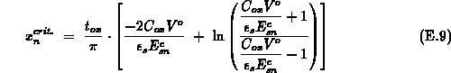
Let us consider the charge-pumping experiments on LDD devices. The interface
areas available for the total carrier capture during the top and bottom level
of the gate pulse are determined by the critical carrier concentrations
 and
and  , respectively. The critical surface fields
 and
and  which are necessary to induce these
concentrations, are given by replacing
which are necessary to induce these
concentrations, are given by replacing  and
and
 according to E.6 in
relationship E.5. For the ranges of interest
according to E.6 in
relationship E.5. For the ranges of interest  and
and
 , which imply
  , after simplifying we get
For discussion later, we advert that the ratio of the fields becomes
 in common cases. The critical coordinate
 follows from E.4, being
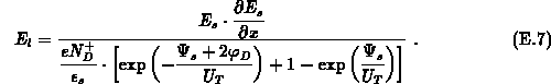
for the electron capture and equivalently with E.9 for the
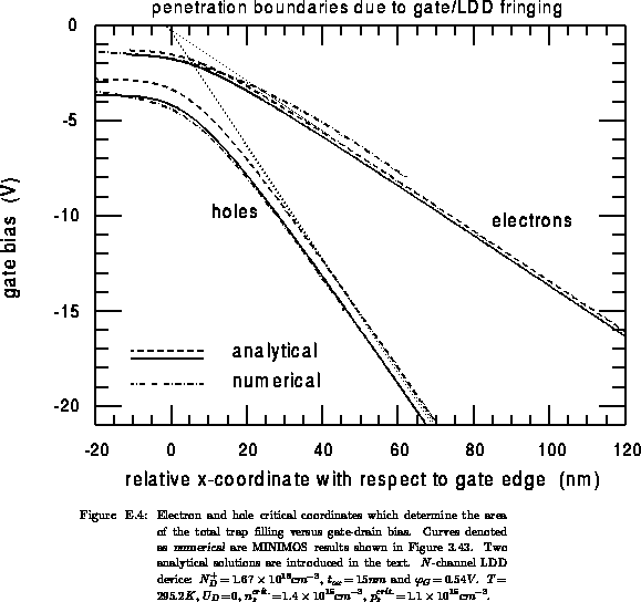
hole capture. Figure E.4 shows the critical electron and hole
coordinates versus gate-drain bias  calculated analytically
by E.9 and numerically by employing MINIMOS (dot-dashed
curves). In real devices, the quantity
calculated analytically
by E.9 and numerically by employing MINIMOS (dot-dashed
curves). In real devices, the quantity  is not constant, but equals to
 , where is the terminal bias,
 the Fermi-level position in the gate and the local surface
potential in the bulk. The dashed line in Figure E.4 represents
the analytical solution when
the Fermi-level position in the gate and the local surface
potential in the bulk. The dashed line in Figure E.4 represents
the analytical solution when  is simply set, whereas the solid
line is the analytical result using
is simply set, whereas the solid
line is the analytical result using
 . For the surface
potential we set the values
. For the surface
potential we set the values  which correspond exactly to
and .
which correspond exactly to
and .
Two observations deserve attention here. The slope
is negative and nearly constant, because of
 ,
which is consistent with Figure E.4. Because
,
which is consistent with Figure E.4. Because  holds, the slope is larger for holes than for electrons. The crossing between
these characteristics determines how far away from the gate edge
one is able to penetrate into the LDD region while scanning interface traps
by using one of the charge-pumping technique. The analytical model shows that
the penetration depth increases almost linearly with the gate-pulse amplitude,
but only moderately with decreasing frequency
(see Figures 3.44 and 3.45).
holds, the slope is larger for holes than for electrons. The crossing between
these characteristics determines how far away from the gate edge
one is able to penetrate into the LDD region while scanning interface traps
by using one of the charge-pumping technique. The analytical model shows that
the penetration depth increases almost linearly with the gate-pulse amplitude,
but only moderately with decreasing frequency
(see Figures 3.44 and 3.45).
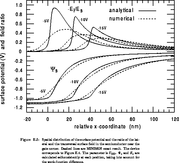
There are deviations of the analytical solution (the solid curve, for the
corrected ) from the numerical solution for electrons in
Figure E.4. In order to explain this result, we have evaluated
the starting assumptions in the derivation of the analytical model. An analysis
for the most critical assumption  is presented in
Figure E.5. The field-ratio is calculated both, numerically and
analytically. For the latter, the ratio is obtained by replacing
is presented in
Figure E.5. The field-ratio is calculated both, numerically and
analytically. For the latter, the ratio is obtained by replacing
 from E.4 in E.7. Both, the
analytical and the numerical approach demonstrate that the induced lateral
field increases to levels comparable with the transversal field in the
semiconductor in the region close to the gate edge. Because of
from E.4 in E.7. Both, the
analytical and the numerical approach demonstrate that the induced lateral
field increases to levels comparable with the transversal field in the
semiconductor in the region close to the gate edge. Because of
 , from the numerical results it follows
that the lateral field never exceeds
, from the numerical results it follows
that the lateral field never exceeds  of the perpendicular
component in the oxide , when
of the perpendicular
component in the oxide , when  . Therefore,
expressions E.2 - E.4 can be judged as being valid,
while the analytical model lost accuracy when solving the Poisson equation near
the gate edge only in one dimension (perpendicular to the interface). Comparing
the surface potential from the analytical and the numerical approach we obtain
that both potentials become close to each other at
. Therefore,
expressions E.2 - E.4 can be judged as being valid,
while the analytical model lost accuracy when solving the Poisson equation near
the gate edge only in one dimension (perpendicular to the interface). Comparing
the surface potential from the analytical and the numerical approach we obtain
that both potentials become close to each other at
 .
This fact explains an excellent agreement between both models for holes in
Figure E.5, since
.
This fact explains an excellent agreement between both models for holes in
Figure E.5, since  . For electrons
 , resulting in the shift to the left with respect to
the numerical results.
, resulting in the shift to the left with respect to
the numerical results.
In the present analysis  and
and
 represent typical values. Although the relative error of the
model depends directly on these parameters, the conclusions we made are valid
for LDD devices in general.
represent typical values. Although the relative error of the
model depends directly on these parameters, the conclusions we made are valid
for LDD devices in general.
An advanced application of this analytical model could be to calculate the QS capacitances due to the gate/LDD fringing effect.
The main drawback of the model presented in this appendix is restriction on the rectangular gates. Thereby, it cannot be employed to model the reoxided gates with an emphasized bird's-beak at the corners. The shape of the gate near the corner is crucially involved at the fringing effect.