We will analyze the first problem in detail. A connection with the second
problem will be established later. When the charge is absent, the potential in
the oxide and bulk, denoted as  , is determined by the two-dimensional
Poisson equation. A localized interface charge induces a perturbation
, is determined by the two-dimensional
Poisson equation. A localized interface charge induces a perturbation  in
the system. Considering the perturbation to be small, the Poisson equation
enables that a relationship
in
the system. Considering the perturbation to be small, the Poisson equation
enables that a relationship
may be written for the bulk. We assume  -type bulk, uniformly doped in
concentration
-type bulk, uniformly doped in
concentration  , with a neutral hole concentration
  ;
;
 . As clarified above, we further adopt the total
depletion approximation. Equation F.1 simplifies to the
Laplace equation which also holds in the oxide. Having the interface charge,
the problem consists of solving the equation
. As clarified above, we further adopt the total
depletion approximation. Equation F.1 simplifies to the
Laplace equation which also holds in the oxide. Having the interface charge,
the problem consists of solving the equation
in the interval  ,
,  , with the
permittivity
, with the
permittivity  for
for  and
and
 when
when  .
.  is the surface charge
density in the plane
is the surface charge
density in the plane  . The problem with the coordinate system is shown
in Figure F.1. The interface charge is distributed in the interval
. The problem with the coordinate system is shown
in Figure F.1. The interface charge is distributed in the interval
 in a space charge density of
 . The boundary condition is
  at
the gate contact. For the sake of simplicity we adopt that the interface charge
does not modulate the local depletion region width
at
the gate contact. For the sake of simplicity we adopt that the interface charge
does not modulate the local depletion region width  (the is connected
with the distribution of ). It follows that
(the is connected
with the distribution of ). It follows that  holds. To
solve the problem one may apply the superposition theorem [375].
Let
holds. To
solve the problem one may apply the superposition theorem [375].
Let  denotes the charge at the position
  :
:
 . This charge induces a potential
  at a particular point
  . The total potential at the point
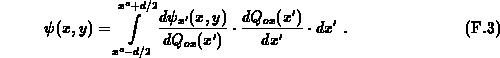
 , induced by the whole interface charge-sheet, is given by
Note that we have to solve a two-dimensional problem; the conditions shown in
Figure F.1 extend in the  -coordinate to infinity. The potential
perturbation, connected with the line charge with strength
-coordinate to infinity. The potential
perturbation, connected with the line charge with strength
 constant in the -direction,
is determined by the equation
constant in the -direction,
is determined by the equation
where we abbreviated  . Equation F.4 is solved in
this work by a standard technique consisting of employing an integral
transformation which converts the primary equation to a simpler
form [311]. Other an approach is to use the method of images. In this
problem we have to consider an infinite number of images in two image-planes,
accounting for the presence of two dielectrics with different permittivity.
. Equation F.4 is solved in
this work by a standard technique consisting of employing an integral
transformation which converts the primary equation to a simpler
form [311]. Other an approach is to use the method of images. In this
problem we have to consider an infinite number of images in two image-planes,
accounting for the presence of two dielectrics with different permittivity.
As integral transformation we choose the Fourier transformation, as done
in [331][40] by solving the three-dimensional point-charge
problem. Here we employ
The local coordinate system used henceforward has its origin in  ,
Figure F.1 (right). Since the problem does not depend on the
-coordinate, the left-hand-side of F.5 yields
,
Figure F.1 (right). Since the problem does not depend on the
-coordinate, the left-hand-side of F.5 yields
Remember that, consistent with F.5,
holds for the Dirac "function" in one dimension. Replacing F.5 into F.6, with benefit of F.7, we obtain
In solving equation F.8 we distinguish three intervals
 ; semiconductor region. The general solution is given with
 , surrounding the
interface at
, surrounding the
interface at  . After one integration of F.8, with benefit
of the continuity of
. After one integration of F.8, with benefit
of the continuity of  and applying
  , we obtain
 ; oxide region. The general solution reads
 it follows:
 and
and  . The unknown coefficients
follow after replacing the latter conditions and the relation of the continuity
of at the interface
. The unknown coefficients
follow after replacing the latter conditions and the relation of the continuity
of at the interface
 in
expressions F.9 - F.11. The solution in the
semiconductor becomes
in
expressions F.9 - F.11. The solution in the
semiconductor becomes
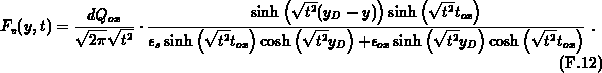
The potential is given with the inverse Fourier transformation
Since 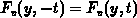 holds for F.12, it
follows
holds for F.12, it
follows
in the half-plane  . An equivalent expression may be written for the oxide.
Although solution F.14 represents only an intermediate step in
our derivation of the total potential perturbation, it is worthwhile to discuss
the qualitative behaviour of this expression. Let us assume a finite
. An equivalent expression may be written for the oxide.
Although solution F.14 represents only an intermediate step in
our derivation of the total potential perturbation, it is worthwhile to discuss
the qualitative behaviour of this expression. Let us assume a finite  and . Solution F.14 exists for all
  , as well at
 and
and  , while it does not exist in the origin ,
  , where
the source of the field is placed, as can be easily concluded by analyzing the
behaviour of the subintegral function for
, where
the source of the field is placed, as can be easily concluded by analyzing the
behaviour of the subintegral function for
 and
and 
 . Note that the
solution to the three-dimensional point-charge problem, where the point
charge is located at the oxide/bulk interface, has equivalent properties. If
. Note that the
solution to the three-dimensional point-charge problem, where the point
charge is located at the oxide/bulk interface, has equivalent properties. If
 , but is finite, solution F.14 exists
in all points except the origin . Particularly, on the
, but is finite, solution F.14 exists
in all points except the origin . Particularly, on the  axis
connected with , it is given in explicit form by
axis
connected with , it is given in explicit form by
For the three-dimensional point-charge problem we found in this case

while the solution does not exist at . If both, and
 the integral in F.14 diverges for all and
, while for the three-dimensional point-charge problem the expression we
derived reduces to the Coulombic potential form:
the integral in F.14 diverges for all and
, while for the three-dimensional point-charge problem the expression we
derived reduces to the Coulombic potential form:
 .
For these special cases the solutions are known from elementary courses.
.
For these special cases the solutions are known from elementary courses.
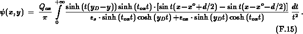
Replacing  from F.14 in F.3, after
an integration with respect to , one obtains the total potential at an
arbitrary point in the bulk induced by the whole charge-sheet at
the interface
from F.14 in F.3, after
an integration with respect to , one obtains the total potential at an
arbitrary point in the bulk induced by the whole charge-sheet at
the interface
For simplicity, but without much loss of generality, a uniform charge density
 is assumed for F.15. In order to prove the
integrability of F.15 let us consider the subintegral function
is assumed for F.15. In order to prove the
integrability of F.15 let us consider the subintegral function
 :
:
 , which is a finite value.
 .
.
Since 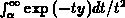 is convergent for all
  when
when  and is a continuous function, the integral
in F.15 is convergent. Moreover, it has a finite value for
and is a continuous function, the integral
in F.15 is convergent. Moreover, it has a finite value for
 and
and  (in the origin), where we are interested to calculate
the surface-potential perturbation. As a conclusion, F.15 exists
everywhere.
(in the origin), where we are interested to calculate
the surface-potential perturbation. As a conclusion, F.15 exists
everywhere.
We focus on the solution at the oxide/bulk interface  , at the middle of
the charge distribution
, at the middle of
the charge distribution  . To further simplify the result let us
suppose that
. To further simplify the result let us
suppose that  . This condition is fulfilled in depletion and
inversion in common cases. Setting , one obtains
. This condition is fulfilled in depletion and
inversion in common cases. Setting , one obtains
with  and the reciprocal effective permittivity for the
oxide/semiconductor system
and the reciprocal effective permittivity for the
oxide/semiconductor system
 .
.
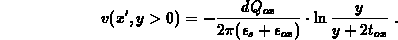
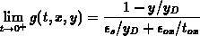
When the charge-sheet extends to infinity, formulae F.15
and F.16 should provide the known relationships. To check this, we
apply  on F.15. Taking advantage of the relationship
and the evenness of  , expression F.15 reduces to
At the interface,
 ;
the charge
;
the charge  is stored in two capacitors, oxide and bulk, connected in
parallel. For we get
is stored in two capacitors, oxide and bulk, connected in
parallel. For we get  , as expected. This
result holds when applying on F.16, as well.
, as expected. This
result holds when applying on F.16, as well.
It is not a trivial task to calculate  in F.16. An
approach, by which many aberrations can be avoided, is to employ the expansion
in F.16. An
approach, by which many aberrations can be avoided, is to employ the expansion
Because of  , this series converges for
  . Taking advantage
of F.18 and using an intermediate result from [152]
(3.945-3), one arrives finally at
. Taking advantage
of F.18 and using an intermediate result from [152]
(3.945-3), one arrives finally at
Note that the case  has been analyzed separately. The series representation
in F.19 converges efficiently and together with F.16
represents the model for the surface band-bending in the middle of the localized
uniform charge, when the depletion region width is large.
has been analyzed separately. The series representation
in F.19 converges efficiently and together with F.16
represents the model for the surface band-bending in the middle of the localized
uniform charge, when the depletion region width is large.
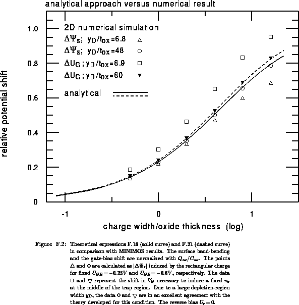
The potential of the theoretical formulation is confirmed by a comparison with
the exact two-dimensional numerical solution, Figure F.2. The
numerical results are computed by MINIMOS, assuming an  -channel
MOSFET with uniformly doped bulk and long channel (
-channel
MOSFET with uniformly doped bulk and long channel ( ). The
localized fixed interface charge is placed in the middle of the channel, thus
avoiding an accidental impact of the source and drain junctions.
). The
localized fixed interface charge is placed in the middle of the channel, thus
avoiding an accidental impact of the source and drain junctions.
In two calculations, we fixed the gate voltage so that the bulk was in depletion
and then we calculated changes in the surface potential at the middle of the
trap-region; the results are  points shown in
Figure F.2. For the data sets, denoted as
points shown in
Figure F.2. For the data sets, denoted as  , the
gate bias has been adapted to establish a surface electron concentration
of
, the
gate bias has been adapted to establish a surface electron concentration
of  at the middle of the trap region. Therefore
 is kept constant for all points in the latter
cases. While the former data sets (
is kept constant for all points in the latter
cases. While the former data sets ( ,
,
 ) correspond to the problem 1, the latter (
 ,
,
 ) represent the problem 2, mentioned at the beginning. The
calculations are carried out for
) represent the problem 2, mentioned at the beginning. The
calculations are carried out for  and
and  , with
no significant effect of on the results. Since a positive charge of
induces a large band-bending of several hundreds
, with
no significant effect of on the results. Since a positive charge of
induces a large band-bending of several hundreds  , care
has been taken to ensure that the bulk was in depletion for all points. For
and data the bulk dopant concentration was
, care
has been taken to ensure that the bulk was in depletion for all points. For
and data the bulk dopant concentration was
 , whereas for and
data we assumed a low concentration of
, whereas for and
data we assumed a low concentration of 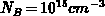 to remove the
depletion region edge away from the interface. The corresponding depletion width
to remove the
depletion region edge away from the interface. The corresponding depletion width
 (where
  being
with respect to potential deep in the bulk) is calculated to be
being
with respect to potential deep in the bulk) is calculated to be  ,
,
 ,
,  and
and  for , , and
data sets, respectively. Solid line represents the analytical
model for an infinitely large , given
by F.16 and F.19. The dashed line is the theoretical
result for expressed by F.21, as will be explained.
All results in Figure F.2 are absolute values normalized
with . Since the ratio
for , , and
data sets, respectively. Solid line represents the analytical
model for an infinitely large , given
by F.16 and F.19. The dashed line is the theoretical
result for expressed by F.21, as will be explained.
All results in Figure F.2 are absolute values normalized
with . Since the ratio  is large for
numerical data, the agreement between numerical and theoretical approaches is
excellent. Small differences come out from a finite in the numerical
calculation, because F.16 is strictly valid if . For
a finite the analytical model is given by F.15, but no simple
analytical solution of this integral has been developed up to now. The
numerical modeling ( points) shows that a finite tends to
reduce the surface band-bending, but only moderately. In fact, the extreme value
of
is large for
numerical data, the agreement between numerical and theoretical approaches is
excellent. Small differences come out from a finite in the numerical
calculation, because F.16 is strictly valid if . For
a finite the analytical model is given by F.15, but no simple
analytical solution of this integral has been developed up to now. The
numerical modeling ( points) shows that a finite tends to
reduce the surface band-bending, but only moderately. In fact, the extreme value
of  is not , but
  which is
less. The total effect of a finite is to increase the surface band
bending with respect to its extreme value, as is clarified below.
which is
less. The total effect of a finite is to increase the surface band
bending with respect to its extreme value, as is clarified below.