2.6 Capacitance Voltage Profiling
Since in a semiconductor the local carrier density depends on the position of
the Fermi level, and hence on the local electrostatic potential, even a
simple parallel plate capacitor structure with one plate replaced by a bulk
semiconductor (MOS) exhibits strongly non-linear behavior [10, 52]. The
charge distribution of minority and majority carriers in such a MOS
structure varies as a function of the applied gate voltage. Depending on this
charge distribution, different operating regimes can be identified. When
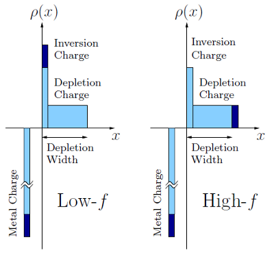
going from accumulation towards inversion, the depletion region inside
the semiconductor is formed first. Here, the majority carriers are driven
away from the interface between the oxide and the semiconductor. The
only remaining charges within this depletion region are fixed ionized
acceptors (p-type) or donors (n-type), which build up a depletion charge. In
combination with the insulator this results in a decrease of the total
capacitance.
With the onset of inversion the minority carriers exceed the majority carriers
at the interface and create the inversion layer. At that point the depletion region
with its ionized impurities virtually stops to increase in width and any increase in
gate charge is only balanced by an increase of the inversion charge. Whether
the minority carriers are able to follow the signal or not influences the
capacitance in this inversion regime, i.e. the contribution of the inversion
layer charge to the total capacitance depends on the frequency. Only
at low frequencies the recombination-generation rates of the minority
carriers can keep up with small signal variations leading to a charge
exchange with the inversion layer. With this additional inversion charge the
capacitance signal increases as the depletion width remains constant [10]. At
high frequencies on the other hand only the majority carrier response
is measured. Hence the incremental charge in deeper inversion is put
at the edge of the depletion region, while the inversion regime is not
altered. This causes the capacitance to remain constant when going from
depletion into inversion. Both cases (low and high frequency) are depicted in
Fig. 2.11.
When adding source and drain regions to form a MOSFET,
minority carriers are provided independently of the frequency. Therefore
low-frequency  -characteristics of MOSCAPs and
  -characteristics
of MOSFETs look alike. Exemplarily, a
-characteristics
of MOSFETs look alike. Exemplarily, a  -characteristics of
a pMOSFET measured at
-characteristics of
a pMOSFET measured at  is depicted in Fig. 2.12. For a
better understanding the curve shown is shifted by the flatband
voltage
and the different operation regimes of the MOSFET are marked.
is depicted in Fig. 2.12. For a
better understanding the curve shown is shifted by the flatband
voltage
and the different operation regimes of the MOSFET are marked.
Based on the above mentioned findings the  -characteristic provides
valuable information of the semiconductor structure and its interface. For
example, present interface states stretch the
-characteristic provides
valuable information of the semiconductor structure and its interface. For
example, present interface states stretch the  -characteristic along the
 -axis, because additional charge is necessary to fill these traps. Oxide charges
on the other hand are independent of the applied
-axis, because additional charge is necessary to fill these traps. Oxide charges
on the other hand are independent of the applied  and cause a mere parallel
shift of the
and cause a mere parallel
shift of the  -characteristic towards higher or lower
  [10]. Furthermore,
with the knowledge of the capacitance as a function of
[10]. Furthermore,
with the knowledge of the capacitance as a function of  , the oxide electric
field can be calculated. This is necessary when the degradation caused by
NBTI is compared with that caused by PBTI for the same device type,
e.g. for a pMOS. Due to the nonzero flatband voltage it is not possible
to apply just the opposite
, the oxide electric
field can be calculated. This is necessary when the degradation caused by
NBTI is compared with that caused by PBTI for the same device type,
e.g. for a pMOS. Due to the nonzero flatband voltage it is not possible
to apply just the opposite  to achieve the opposite electric field.
Moreover, the different behavior of the capacitance during accumulation
and inversion yields an asymmetric
to achieve the opposite electric field.
Moreover, the different behavior of the capacitance during accumulation
and inversion yields an asymmetric  -characteristic. This as well
influences the value of the proper (exact opposite) field. An application
of
-characteristic. This as well
influences the value of the proper (exact opposite) field. An application
of  -characteristics to obtain the required stress voltage
  for a certain NBTI stress and its corresponding PBTI stress is given in
Chapter 7.
for a certain NBTI stress and its corresponding PBTI stress is given in
Chapter 7.
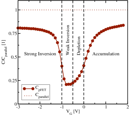
 -curve of a pMOSFET taken at
  and
normalized to the capacitance of an ideal capacitor of the same size. To
be able to distinguish between the different operating regimes more easily,
the graph is also shifted by the workfunction difference. The flatband
capacitance
and
normalized to the capacitance of an ideal capacitor of the same size. To
be able to distinguish between the different operating regimes more easily,
the graph is also shifted by the workfunction difference. The flatband
capacitance  is then obtained at
  .
.