6.3.5 Extracted Prefactors
The prefactor  of the log-fit for various
  ,
,  , and
, and  is displayed in
Fig. 6.13. In agreement with previous experiments, it is observed that low
is displayed in
Fig. 6.13. In agreement with previous experiments, it is observed that low
 results in small temperature activation, while
  larger than the
operating voltage of the MOSFET gives a notable activation energy of
larger than the
operating voltage of the MOSFET gives a notable activation energy of  .
Note that this value is in agreement with activation energies extracted at long
stress times [106]. Fitting the data to a power-law
.
Note that this value is in agreement with activation energies extracted at long
stress times [106]. Fitting the data to a power-law  results in an
exponent
results in an
exponent  for short-term stress, roughly a third of the often reported
 of the long-term behavior. This is in very good accordance with the
standard
of the long-term behavior. This is in very good accordance with the
standard  for NBTI stress and accounts for a strong
  dependence,
excluding elastic hole tunneling.
dependence,
excluding elastic hole tunneling.
Figure 6.14 represents the prefactor  plotted for different
  at different
temperatures. In the devices with
at different
temperatures. In the devices with  , all the stress voltages
are above the operating voltage and result in a marked temperature
activation. For
, all the stress voltages
are above the operating voltage and result in a marked temperature
activation. For  the transition from no temperature activation
to temperature activation is observed between
the transition from no temperature activation
to temperature activation is observed between  and
and
 for
for  . For the thickest oxides used in this study,
 , the applied stress fields are too small to lead to a meaningful
degradation .
Therefore no objective statement can be made on temperature activation
concerning the here presented devices with
, the applied stress fields are too small to lead to a meaningful
degradation .
Therefore no objective statement can be made on temperature activation
concerning the here presented devices with  .
.
However, the experiments performed on devices with smaller oxide
thicknesses support thermally activated tunneling mechanism [98] rather than
elastic (and thus temperature-independent) hole tunneling [94].
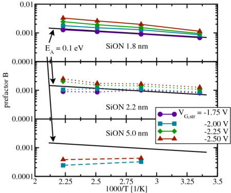
 of the log-fit, extracted
from three different
of the log-fit, extracted
from three different  for different
  . An activation energy
  of
about
of
about  is obtained for
  and
and  , represented
by the black solid line. Degradation for the
, represented
by the black solid line. Degradation for the  devices was too
noisy due to too low
devices was too
noisy due to too low  . Scale is equal for all plots.
 of the log-fit plotted for different
  with
different temperature
with
different temperature  . While
  shows a clear temperature
activation,
shows a clear temperature
activation,  does not due to the low electric stress field. For
 the transition of the temperature dependence is visible at
 between
  and
and  .
.