Previous: 6.1 Historical Overview Up: 6. Introduction Next: 6.3 Outline of the First Part
 |
In the mid-1970s down-scaling of MOS devices was started aggressively. Soon the dimensions of the transistors reached a point where simple physical models of dopant distribution and device behavior were not valid any longer. It was noted that it is necessary to understand the coupling between process conditions, the electromagnetic behavior of the devices, and the performance of the resulting integrated circuit.
Thus as more ambitious devices were designed and fabricated, it became apparent that computer simulations would play a crucial role in the development of this new technology. Computer simulations made it possible to understand related process and device effects. Furthermore, their great advantages compared to the experimental approach are the rapid turn-around time and the much lower cost.
Computer experiments based on suitable, adjusted models can be carried out much faster than manufacturing expensive test structures and they enable to find many properties of the devices in an early stage of the development process of new technologies. Furthermore the understanding of the physical processes which occur during the fabrication and the operation of the devices is deepened. Hence, using predictive simulations, devices can be optimized in an early phase and the manufacturing processes can be improved not only with respect to the quality of the resulting devices, but also with respect to manufacturing throughput.
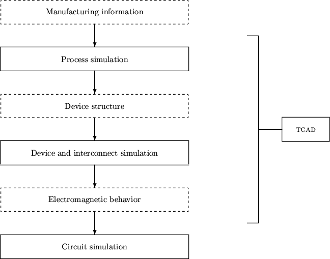
The term TCAD (technology computer aided design) is used for simulations in the field of semiconductor device manufacturing and its scope is explained in Figure 6.1 [114]. Information about the manufacturing steps and conditions are used for simulating the various processes. The resulting geometric description of the device structure provides the input for the simulation of the electromagnetic behavior of the device and the interconnects. Finally the characteristic behavior of the device or compact models thereof are used for the simulation of the integrated circuit. Thus TCAD means the derivation and investigation of models of semiconductor processes and devices and the simulation based on these models, but it does not include circuit simulation.
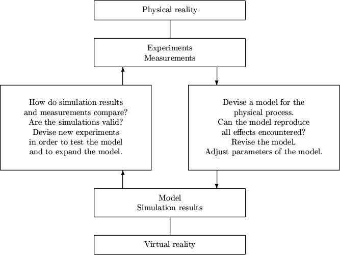
Figure 6.2 depicts the relationship between our physical reality, i.e., experiments that are carried out, and the virtual reality of modeling and simulation. First of all experiments capturing the essential part of the process considered are devised and carried out, and thus measurements are obtained. Then a model of this physical process is devised. It should be able to reproduce all effects encountered. In the next step the model is evaluated for certain situations, i.e., simulations are carried out. This may lead to substantial numerical calculations and this is usually the case in the field of TCAD.
The simulation results are compared to measurements initially obtained. Are the simulations valid? Do they properly reproduce the phenomena observed? Are all important effects accounted for? Depending on these questions new experiments are devised in order to test the model or to expand the model to properly include all necessary effects.
This cycle is usually repeated several times until the simulations satisfactorily agree with reality. Here the right balance between the accuracy of the model, its complexity, and its usefulness for theoretic and practical purposes has to be found. The preciser the model becomes, the longer evaluations take in general. Depending on the purpose of the simulations a simpler model reproducing and explaining the essential effects may be preferable. Properties of solutions to model equations like their asymptotic behavior may be seen in a straightforward manner in a simpler formulation of the model. Often it is also useful to compare versions of the same model in order to determine the cause of a single effect.
The simulation of manufacturing processes and the electromagnetic activities in today's semiconductor devices is one of the most demanding and exciting subjects in electronics and applied mathematics. A large variety of problems in modeling physical and chemical processes and in numerics must be solved in order to obtain predictive simulations.
However, in order to arrive at predictive simulations it is indispensable to continuously review the models and to determine the values of parameters the model may depend on as precisely as possible. The second problem is commonly referred to as inverse modeling or parameter extraction. Solving it in order to increase the accuracy of simulations and making them more predictive is crucial for real world applications and it ought to be done whenever new measurements are available (cf. Figure 6.2). In the second part of this thesis new impulses to solving this problem in practice are presented and these methods were applied to several inverse modeling and optimization problems of practical importance.
Clemens Heitzinger 2003-05-08