Ion implantation has turned out to be the best suited technique to selectively introduce dopants into semiconductor materials. To perform ion implantation a focused ion beam containing just one particle species (atom, molecule or atom cluster) with a well defined energy is required. Ionized particles are used because they can be easily accelerated and there is an efficient way for the separation of ionized particle species.
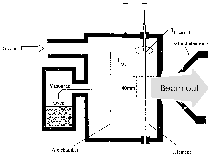
The ions are generated in an ion source which consists of an oven where the particles are vaporized, and the arc chamber, where the particles are ionized mainly by the bombardment of the atoms or molecules with electrons but also by atom/atom and atom/molecule collisions. Due to a well designed magnetic field in the arc chamber, which increases the path length of the electrons, and by the external generation of electrons, the electron/atom collision probability is increased, enabling a larger ion density. Fig. 2.1 shows one example of an ion source, a schematic description of a Harwell Freeman ion source [91].
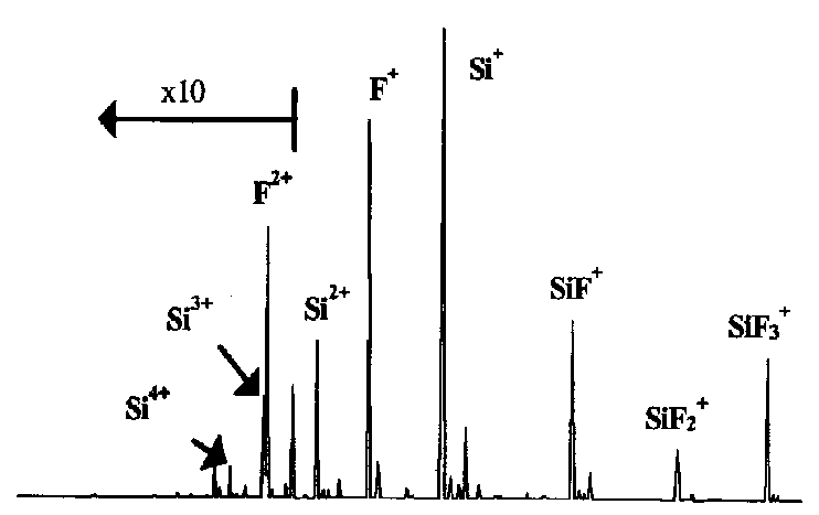
There are various types of ion sources differing in the design of the arc chamber and in the electron generation method.The ion beam which leaves the particle source is divergent. It is focused by an electric or magnetic field lens to avoid ion loss to the wall of the beam line and to ensure that the ion beam reaches the wafer in a reasonably well defined focus. After leaving the ion source the beam contains a lot of atom and molecule species in several charge states. Fig. 2.2 shows a typical ion source beam spectrum.
The desired dopant is separated from the remaining elements by an analyzing magnet. Thereby it is made use of the physical effect that charged particles trace circular orbits with a radius proportional to the ratio of the mass and the charge, when passing through a uniform magnetic field. An initial beam containing various particle species can thereby be split into several single species beams with different beam directions, so that a small aperture placed behind the analyzing magnet can absorb all but one particle species. The remaining ions are accelerated to the required energy, before they reach the process chamber where one or several wafers are located.
Due to the fact that the area covered by the ion beam has a size of typically
some cm![]() the beam has to be scanned across the wafer to guarantee a uniform
implantation dose for the whole wafer which has a diameter of up to
300 mm. Electrostatic beam scanning, magnetic beam scanning, linear mechanical
beam scanning, spinning disk techniques or a combination of these techniques are
applied [91]. Even if electrostatic or magnetic beam scanning are
technically less complicated they usually suffer from the problem that the angle
of incidence of the ion beam (tilt angle) on the wafer varies across the wafer
up to some degrees. This results in non-uniform doping profiles across the
wafer, because the penetration depth of the ions is very sensitive to the tilt
angle. Recently electrostatic scanning systems have be developed which
compensate these tilt angle variations.
the beam has to be scanned across the wafer to guarantee a uniform
implantation dose for the whole wafer which has a diameter of up to
300 mm. Electrostatic beam scanning, magnetic beam scanning, linear mechanical
beam scanning, spinning disk techniques or a combination of these techniques are
applied [91]. Even if electrostatic or magnetic beam scanning are
technically less complicated they usually suffer from the problem that the angle
of incidence of the ion beam (tilt angle) on the wafer varies across the wafer
up to some degrees. This results in non-uniform doping profiles across the
wafer, because the penetration depth of the ions is very sensitive to the tilt
angle. Recently electrostatic scanning systems have be developed which
compensate these tilt angle variations.
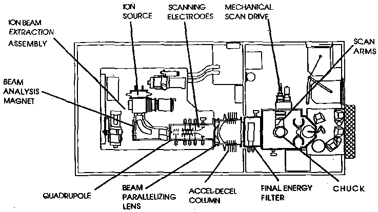
As an example for an implanter a schematic description of the medium current implanter Eaton NV8200 is shown in Fig. 2.3. The ions are generated in the ions source, a single particle species beam is extracted by the beam analysis magnet and focused by a quadrupole double lens [91]. By the scanning electrodes the ion beam is scanned horizontally (x-axis) into a fan-shaped pattern, which is subsequently angle corrected into a ribbon shaped pattern by the beam parallelizing lens. Finally the ion beam is accelerated to the required implantation energy in the accel-decel column and deflected towards the wafer surface by the final energy filter which guarantees a mono-energetic ion beam. A mechanical scanning system performs the y-axis scanning.
![]()
![]()
![]()
![]() Previous: 2. Ion Implantation Technology
Up: 2. Ion Implantation Technology
Next: 2.2 Ion Implantation Process
Previous: 2. Ion Implantation Technology
Up: 2. Ion Implantation Technology
Next: 2.2 Ion Implantation Process