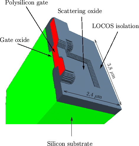
Fig. 5.26 shows the input structure for the ion implantation. It is one half of an NMOS-Transistor, which is cut through the gate. The crystalline silicon substrate is partly covered by a thick silicon dioxide layer forming the isolation and a thin silicon dioxide layer serving as the gate oxide and as a scattering oxide for the implantation. The gate is made of polysilicon which is also covered by a thin silicon dioxide layer.
 |
By this implantation a heavily n-type doped region is formed in the p-type substrate. Due to this counter doping, diodes are formed between the gate and the source area and the gate and the drain area. Thereby the source area is electrically isolated from the drain area because one of these diodes is always reverse biased and the transistor can only be made conductive by applying a voltage at the gate to inverse a thin layer below the gate.
The implantation is performed with arsenic ions with an energy of 90 keV and a
dose of
![]() cm
cm![]() . The ion beam is tilted by 7
. The ion beam is tilted by 7
![]() and rotated by
0
and rotated by
0
![]() . An
arsenic concentration of up to
. An
arsenic concentration of up to
![]() cm
cm![]() is introduced into the substrate by
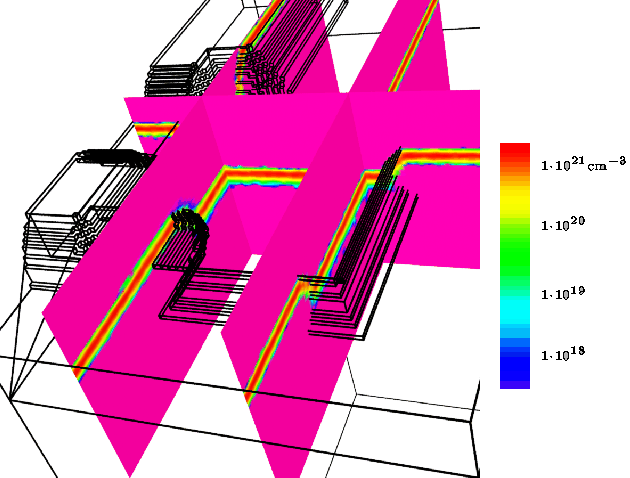
this implantation as shown in Fig. 5.27. To give an impression of the
three-dimensional simulation result the arsenic distribution is show in three
cuts through the source/drain region in common with an outline of the transistor
structure.
is introduced into the substrate by
this implantation as shown in Fig. 5.27. To give an impression of the
three-dimensional simulation result the arsenic distribution is show in three
cuts through the source/drain region in common with an outline of the transistor
structure.
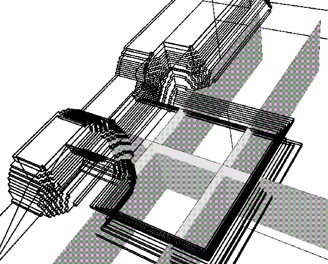
Due to the high implantation dose a part of the active area becomes amorphous. As shown in Fig. 5.28, in the silicon substrate below the source/drain region a 10 nm thick amorphous layer is formed. During the following annealing step this amorphous layer is converted back to crystalline silicon. Worth mentioning is that the recrystallization process of amorphous zones is a faster process than the annealing process of isolated point defects in silicon. Therefore shorter annealing times can be used for the activation of the dopant atoms if amorphous layers are formed during implantation.
Like the arsenic distribution, the amorphous zones are visualized within three cuts through the source/drain region in Fig. 5.28. 1500000 distinct ions were simulated applying the Follow-Each-Recoil method. This simulation required about 40 hours of CPU-time on a DEC-600 workstation with 333 MHz CPU clock frequency.
 |
 |
![]()
![]()
![]()
![]() Previous: 5.4.1 Threshold Voltage Adjust
Up: 5.4 Implantation into Topological
Next: 6. Conclusion and Outlook
Previous: 5.4.1 Threshold Voltage Adjust
Up: 5.4 Implantation into Topological
Next: 6. Conclusion and Outlook