Next: 9. Intrinsic Stress Effects
Up: 8. Thermo-Mechanical Stress in
Previous: 8.1 Simulation Procedure
Subsections
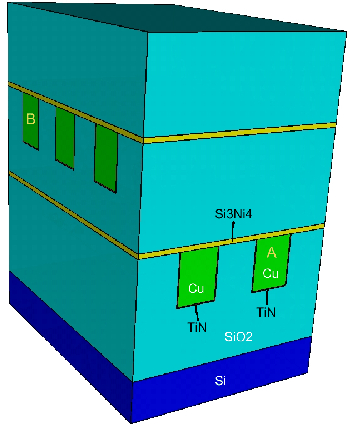
A three-dimensional interconnect layout with (3.0 4.2)
4.2) m floor space, as displayed in Fig. 8.2, is investigated by the two previously defined models. In this structure the bottom layer material is silicon (Si). Above the silicon layer there is a silicon dioxide (SiO
 ) layer, where two copper (Cu) lines are embedded. Between the copper lines and the silicon dioxide is a very thin titanium nitride (TiN) passiviation layer. This passiviation layer prevents the diffusion of copper into the silicon dioxide during the manufacturing process [128].
As shown in Fig. 8.2, the silicon dioxide layer and the copper lines are covered by a silicon nitride (Si N
N ) layer which separates the next upper located SiO layer from the lower one.
In the second upper SiO layer three copper lines are embedded. These three copper lines are transverse compared to the two subjacent copper lines. This upper SiO layer is also covered with silicon nitride. On the top of the layout is a third SiO layer.
) layer which separates the next upper located SiO layer from the lower one.
In the second upper SiO layer three copper lines are embedded. These three copper lines are transverse compared to the two subjacent copper lines. This upper SiO layer is also covered with silicon nitride. On the top of the layout is a third SiO layer.
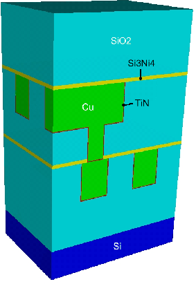
In Fig. 8.3 a cut through the interconnect structure given in Fig. 8.2 is presented. As evident from Fig. 8.3 an upper transverse copper line is connected with a lower copper line by a so-called via. The other two copper lines shown in this figure are connected in the same way. The third transverse upper copper line (see Fig. 8.2) does not have an interconnection to another line.
Figure 8.2:
Investigated complete interconnect structure.
|
|
Figure 8.3:
Cut through the interconnect layout.
|
|
From the simulation aspect the temperature and stress distribution in the given interconnect structure at two different points of time are of interest. For the simulation a potential difference of 7mV between point A and B in the first interconnect, as marked in Fig. 8.2, is assumed. The other interconnects are assumed to be inactive.
If STAP with its electro-thermal model is applied to this interconnect structure, the obtained output is the temperature distribution in the structure. In this analysis it is assumed that the bottom of the silicon layer is connected with a cooling element which holds the temperature at 320K. For the simulation the electric and thermal conductivities given in Table 8.1 are used. Because copper is a metal and an excellent conductor, it has the best thermal and electric conductivity regarding feasible materials for interconnect metals.
Table 8.1:
Electric and thermal conductivities at 300 K [129].
| |
Cu |
Si |
SiO |
SiN |
TiN |
 [S/m] [S/m] |
5.26 x 10 |
0.0 |
0.0 |
0.0 |
1.66 x 10 |
 [W/mK] [W/mK] |
400.0 |
1.35 |
1.39 |
12.07 |
48.25 |
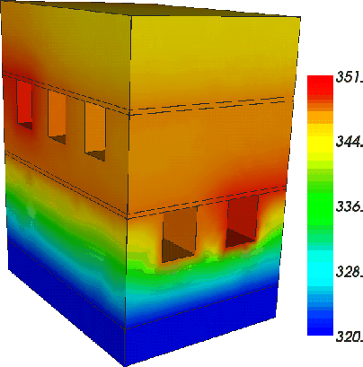
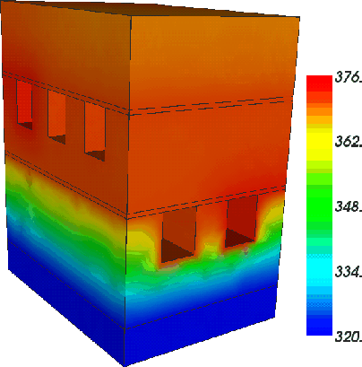
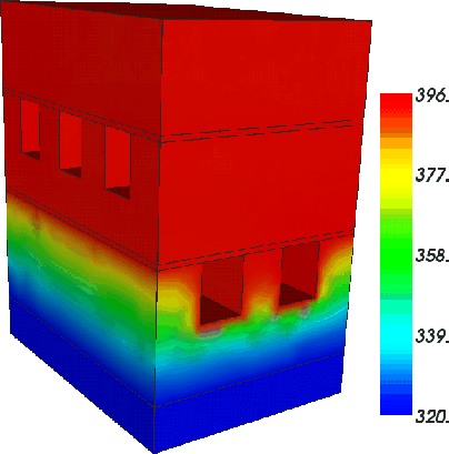
Due to the Joule self-heating in wires with a current flow, the hottest regions are around the active copper line. This is the reason, why after a time of 30s the highest temperature (351K) is in the inner layers which are surrounded by the active copper line, as shown in Fig. 8.4. The relatively high thermal conductivity of copper causes that the temperature values in the copper lines are rather uniform, and so they are not included in Fig. 8.4. In Fig. 8.5 it is demonstrated that after a longer operating time of 100s the self-heating has increased the temperature to 376K.
In Fig. 8.7 the maximal temperature versus operating time in the interconnect structure is plotted. It can be seen that after approximately 450s the self heating effect reaches a stable steady state.
Fig. 8.6 shows the temperature distribution in the steady state where the maximal temperature has reached a steady value of 396K.
Figure 8.7:
Maximal temperature versus time in the interconnect structure.
|
|
For the pressure calculation, the influence of the temperature on the mechanical parameters can be neglected, because the temperatures are so low that they do not change the material condition perceivably [130]. Also the influence of pressure on the electric and thermal parameters can be neglected for such pressure values [131]. Therefore, a coupling of the electro-thermal and thermo-mechanical system is not necessary and the decoupled alternating solving of the temperature and pressure distribution is acceptable here. With the obtained temperature distribution the mechanical problem can be set up as described in Section 8.1.2. As applied mechanical boundary conditions the bottom surface is fixed and the other surfaces are free. For the simulation the Young modulus E, Poisson ratio  , and the thermal expansion factor
  given in Table 8.2 are used.
Table 8.2:
Mechanical parameters
| |
Cu |
Si |
SiO |
SiN |
TiN |
| E [GPa] |
115 |
180 |
73 |
380 |
600 |
| [-] |
0.34 |
0.22 |
0.17 |
0.27 |
0.25 |
[10 /K] /K] |
17.7 |
2.7 |
0.55 |
3.3 |
9.4 |
The distribution of pressure is an important quantity for electromigration, because failure risks are increasing with larger pressure. Therefore, the copper lines and their vias are the most interesting regions. The thermal expansion coefficient of copper is the largest and it is enormous compared with the main embedding material silicon dioxide (see Table 8.2).
This larger coefficient of the copper lines demands more volume expansion than the other surrounding materials in the heated structure. This means that the copper lines with their vias can not expand as desired and compressive stress is built up.
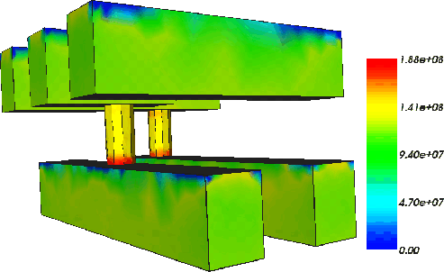
Fig. 8.8 shows the simulation results of the pressure distribution in the copper lines and their vias at time 30s. It can be seen that the via is a high pressure region. The first reason is that the via has less chance to expand in vertical direction because of the over- and underlying copper lines which also have the same demand to extend. The other explanation is the confinement of the via by the passivation layer (see Fig. 8.3) which was made of titanium nitride (TiN). The passivation layer is thin, but the stiffness (Young modulus) of TiN is more than five times larger than the copper one and so this layer is able to prevent the volume increase.
The proof is that the largest pressure (188MPa) develops at the bottom of the vias, because it is confined with the passivation layer. The pressure in the bottom region is larger than on the top, where is no limiting TiN-layer.
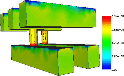
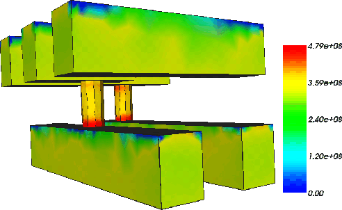
After a longer operating time of 100s the higher temperature in the structure (see Fig. 8.5), causes that the maximum pressure in the via is increased to 354MPa, as displayed in Fig. 8.9. The pressure distribution in the copper lines and vias is nearly the same as at time 30s. As illustrated in Fig. 8.10 the pressure reaches a maximum of 479MPa in the steady state.
Figure 8.8:
Pressure distribution in the copper lines and their vias in Pascal [Pa] at time 30 s.
|
|
Figure 8.9:
Pressure distribution in the copper lines and their vias in Pascal [Pa] at time 100 s.
|
|
Figure 8.10:
Pressure distribution in the copper lines and their vias in Pascal [Pa] in the steady state.
|
|
Next: 9. Intrinsic Stress Effects
Up: 8. Thermo-Mechanical Stress in
Previous: 8.1 Simulation Procedure
Ch. Hollauer: Modeling of Thermal Oxidation and Stress Effects
![\includegraphics[width=0.7\linewidth,bb=29 48 717 528, clip]{interconsim/320K-t-T}](img941.png)