Next: 1.3 Electrical and Physical Up: 1. Introduction Previous: 1.1 Challenges Discussed in Contents
Since the beginning of the microelectronics age, the increase in sophistication of semiconductor devices seems to grow exponentially. This behavior was described by MOORE1.1 [6] in 1965 and remains valid until today [7]. The transistor integration densities as well as the complexity of microelectronic devices have increased in the same speed. On average, they have doubled every eighteen months [8,9,10,11,3]. This observation has become known as MOORE's law.
It seems that despite some fluctuations of the average speed of the enhancements, the growth rate remains exponential and keeps constant for microprocessors and memory and seems to remain valid for future devices [7]. At present, the upcoming challenges are the absolute physical constraints of the atomic material structure [3] in terms of the electrical behavior and mechanical properties due to the high stress gradients in thin film materials which appear during fabrication and may be enhanced during device operation.
The enhancement of integration and the shrinking of the device feature size leads to smaller and more sophisticated devices. Thus, more devices can be integrated within the same area as before, leading to a higher package density. At a certain package density, however, new effects become important, e.g. self-heating of the semiconductor devices and the interconnect lines [11,12]. To overcome these problems, the device engineers have to develop smart device arrangements and new technologies for fabrication to reduce parasitic (thermal) effects or to exploit them by using these effects for compensation purposes.
|
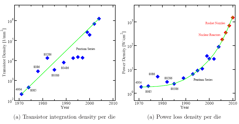
In 1959, the first integrated circuit was presented by KILBY [13,14] which was followed by the first microprocessor on a single chip, the 4004 from INTEL in 1971 [2]. This processor series was improved and continued by the 8008 in 1974 and other processors. In 1978, the 8086 [2] was announced and newer and more powerful processors have followed.
The outlook of MOORE on the future of semiconductors has motivated and forced design and research centers to fulfill the predictions of MOORE. A viewgraph of the achieved enhancements for microprocessors is outlined in Figure 1.1. The current version of the International Technology Roadmap for Semiconductors (ITRS) summarizes the requirements which are mandatory for the future enhancements to obtain the predicted sophistication of semiconductor devices.
Figure 1.1 shows the achievements for microprocessors over the last decades since 1972 [2]. In Figure 1.1a a logarithmic plot shows the transistor density of selected microprocessors versus the year of their announcements. Obviously, the transistor density on die shows an exponential growth. It doubles every 18 months. Figure 1.1b depicts the corresponding power loss densities on these selected microprocessor chips. As it is clearly depicted in Figure 1.1b, the power loss density increases exponentially even on the logarithmic scale. Extrapolated by the current growth rates and assuming that the past trends in development will continue, we would soon reach power loss densities of nuclear power plants or rocket nozzles in a few years.
With the fast development of the early semiconductor technology in terms of purity of the materials, the integration density, and the complexity of the device structures, new processor types have become possible, e.g. the 80286, 80386, 80486, and today Core2Duo and Core2Quad. In 1975, MOORE's forecast of the electrical operation conditions as well as the package density of the processors from the 1980s were assumed to be highly futuristic and not realizable in terms of former device fabrication processes [8]. However, this vision has come true and the processors were realized in spite of general disbelief and are being constantly improved.
Today, a similar development of the enhancement process can be observed.
According to the future predictions of the current ITRS [3], device
structures have been proposed which reach or have already gone beyond of the
absolute physical constraints for classical devices.
For instance, the thicknesses of gate oxides have been successfully reduced to
approximately three to four atomic layers of
![]() [15,16]
(cf. Figure 1.2), which raises questions about the efficiency due to high
leakage currents through these thin layers [17] and long-life
reliability [18].
However, for switching transistors used in digital logic devices, the provided
functionality is sufficient for reliable operation. This point of view is
completely different from ten to twenty years ago, but changing the view point
has enabled engineers to find new solutions within these new constraints.
From our current understanding, shrinking this type of devices by one more step
would result in oxide thicknesses of two atomic layers and the energy
barriers in this structure would be far too small for a proper transistor
operation.
As an alternative to these limits, new materials with
a higher dielectric constant are introduced which provide the same capacitance
as
[15,16]
(cf. Figure 1.2), which raises questions about the efficiency due to high
leakage currents through these thin layers [17] and long-life
reliability [18].
However, for switching transistors used in digital logic devices, the provided
functionality is sufficient for reliable operation. This point of view is
completely different from ten to twenty years ago, but changing the view point
has enabled engineers to find new solutions within these new constraints.
From our current understanding, shrinking this type of devices by one more step
would result in oxide thicknesses of two atomic layers and the energy
barriers in this structure would be far too small for a proper transistor
operation.
As an alternative to these limits, new materials with
a higher dielectric constant are introduced which provide the same capacitance
as
![]() but with a larger gate dielectric thickness.
In order to compare the effective thickness of the gate
dielectric, the physical thickness of the gate dielectrics is mapped to the
thickness of a
but with a larger gate dielectric thickness.
In order to compare the effective thickness of the gate
dielectric, the physical thickness of the gate dielectrics is mapped to the
thickness of a
![]() layer with the same electrical
properties. This thickness is called the effective oxide thickness (EOT).
layer with the same electrical
properties. This thickness is called the effective oxide thickness (EOT).
This example shows the capabilities of how new technologies can exploit certain material properties to enhance the transistor performance and to reduce the area per transistor on a die. In addition, this simple example has shown that the future will bring new paradigms for building and operating electronic devices.