Next: 2.2.5 Heat Sinks and Up: 2.2 Heating Phenomena Previous: 2.2.3 Electro-Magnetic Power Density Contents
Beginning with the local point of view, the heat conduction equation (2.9) determines the behavior at the current position and in a certain small region around the current position. In this environment, the heat is generated, for instance, if charge carriers are forced to move and are accelerated according to an external applied electric field. Hence, also the kinetic energy of the carriers increases. According to elastic and inelastic scattering effects at lattice sites, impurities, and surface areas, parts of the carrier's kinetic energy are converted to heat. Therefore, a temperature can be assigned to charge carriers, where these assigned carrier temperatures directly correspond to their energies but does not correlate with the commonly known thermodynamic temperature. Especially for charge transport in semiconductor materials, the carrier temperature assignments are very common [87] to determine carrier energy (cf. hot and cold electrons in [63,62,72]).
For small carrier flows in semiconductor devices, the semiconductor substrate temperature and therefore also the channel lattice temperature can be assumed to be equal to the ambient temperature, since self-heating is negligible.
To determine the heating effects, especially for interconnect materials, most involved materials can be assumed to behave like metals. Since highly doped semiconductor materials and also silicides have been introduced to interconnect structures and their resistivity can be adjusted within certain ranges, also their electrical behavior is quite similar to that of metals. Hence, these materials can be treated as metal-like materials, or, if special material-specific effects have to be considered, the model can be extended to account for this particular effect. For instance, highly doped tungsten silicide is often used as a conductor. Hence, it is possible to use freely available regions to integrate fusing elements that exploit electro-migration effects in tungsten silicide [88,89,90].
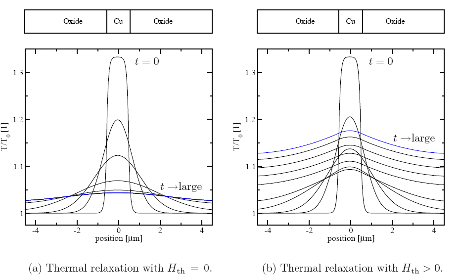
As an illustrating example for heating and cooling, a copper plate
embedded in
![]() dielectrics has been heated up to a certain temperature
and the corresponding cooling procedure is shown in Figure 2.2a.
This figure depicts an undisturbed thermal relaxation (cooling) where
the heat energy and therefore the temperature diffuses to the surrounding
oxide layers to become uniformly distributed over the simulation region.
For the simulations shown in Figure 2.2, adiabatic boundary conditions are
applied where the simulation region does not exchange energy which any other
surrounding systems. This can for instance be assumed if this particular
simulation domain is embedded in a large periodic structure.
In contrast, by considering a continously heated copper plate in Figure 2.2b, the result of
the heat conduction equation (2.9) gives0 the evolution of the
temperature distribution at different points in time with an additional heat
source term
dielectrics has been heated up to a certain temperature
and the corresponding cooling procedure is shown in Figure 2.2a.
This figure depicts an undisturbed thermal relaxation (cooling) where
the heat energy and therefore the temperature diffuses to the surrounding
oxide layers to become uniformly distributed over the simulation region.
For the simulations shown in Figure 2.2, adiabatic boundary conditions are
applied where the simulation region does not exchange energy which any other
surrounding systems. This can for instance be assumed if this particular
simulation domain is embedded in a large periodic structure.
In contrast, by considering a continously heated copper plate in Figure 2.2b, the result of
the heat conduction equation (2.9) gives0 the evolution of the
temperature distribution at different points in time with an additional heat
source term
![]() applied.
The heat becomes distributed over the whole simulation domain, where heat
conduction is the dominant energy transport mechanisms.
Radiation has been neglected in this investigation.
applied.
The heat becomes distributed over the whole simulation domain, where heat
conduction is the dominant energy transport mechanisms.
Radiation has been neglected in this investigation.
|
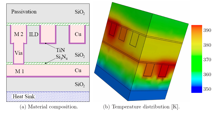
A similar phenomenon can be observed in interconnect structures with included vias. The heat produced by self-heating is preferably transfered through the metal layers and the via structures because the thermal conductivity of the interconnect lines and vias is much higher than those of the barrier layers and the surrounding dielectrics. Since the vias are made of metal and silicided materials, the vias provide a strong secondary heat transfer path in addition to the metal layers, which is often not considered and anticipated appropriately. As a consequence, measurements show that real structures globally heat up during operation and thermal failures may occur which seem to be unmotivated in terms of electrical simulation. With simulators that use suitable thermal models, such possible failures can be identified.
The high supply voltages and increasing clock frequencies are another promoting factor for additional thermal loads because the intervals between the loading and decharging of the intrinsic capacitors are becoming shorter. This requires to operate at higher current densities. In addition, this phenomenon is emphasized when CMOS device structures are considered. During a transition, when the device is turned on or off, both driver transistor are for a short period of time in the on-position. That means, a higher current flows through the devices from the positive supply connector to ground and thus the power loss increases quadratically [91]. This effect can be observed when only frequency scaling is applied for a particular technology.
Rigorous self-consistent electro-thermal investigations of complex interconnect structures have become very time consuming, especially when temperature-dependent material parameters are considered. For these investigations, the three-dimensional interconnect simulator STAP [92,93,39] has been developed to extract resistances, capacitances as well as internal quantity distributions such as potential, current density, and temperature, among others.
As a representative example, a typically multi-layered interconnect structure is
electro-thermally investigated. Figure 2.3a depicts a structure which
consists of several metalization layers which are connected through vias. In
between these metal lines, there is
![]() as an interlayer dielectric
(ILD). The copper lines are coated by
as an interlayer dielectric
(ILD). The copper lines are coated by
![]() barrier layers to avoid copper
diffusion into
barrier layers to avoid copper
diffusion into
![]() . As an etch-stop layer, a
. As an etch-stop layer, a
![]() passivation layer is
included due to technology-induced constraints.
passivation layer is
included due to technology-induced constraints.
|
As Figure 2.3 shows, the electrical load in semiconductor devices and in interconnect structures produces a considerable amount of heat which has to be included into the design of heat sinks. Due to global heating, many interconnect regions become thermally and mechanically stressed even these which are not directly electrically stressed. Therefore, these regions become extraordinary burdened by further electrical or mechanical stressing effects. Hence, the heat metal lines and metalization layers can be used to shield some regions from external heating by providing an additional heat conduction path with a very low thermal resistivity allowing a fast transport path towards a heat sink.