Next: 2.4 Material Deposition Up: 2.3 Material Properties Previous: 2.3.1.4 Barrier Layers Contents
Material properties of polycrystalline materials are often modeled in a similar fashion as single crystals thereby neglecting the internal microstructure. Unfortunately, most of the available deposition technologies only provide polycrystalline or amorphous rather than single crystal deposition. The only deposition process which provides single crystal growth in the processing reactor is the atomic layer deposition (ALD) which provides a very low growth rate and is therefore rather expensive with respect to time. Nevertheless, if crystalline structures have to be used, for instance in semiconducting materials, expensive single crystal deposition or growth methods have to be applied anyways. For most other applications, however, amorphous and polycrystalline regions are sufficient for device operation. For instance a crystalline structure of interconnect lines, contacts, and dielectrics is generally not required. However, the down-scaling of the semiconductor devices has also resulted in a certain downscaling of the interconnect structures. With lower line dimensions, however, additional effects which need to be negligible have now to be considered as well. For instance the grain boundaries of all polycrystalline materials contain unsaturated bounds, which can bind impurities. As a consequence energetic barriers form at these sites. Another crucial effect is the enhanced diffusion due to a lowering of the activation energy at these grain boundaries and material interfaces.
Typical properties of grain boundaries are that they have higher thermal conductivity than the surrounding material [161]. In addition, they can also have a higher melting point than the bulk material because there may exist some constellations (phase stages) where the grain boundary regions have higher thermal stability than the surrounding bulk-like material and can therefore act as a stabilizing element in the material structure [161]. If these stabilizing grain boundary elements are located in a material with a certain regular density, they mainly determine the behavior of high temperature regions.
 |
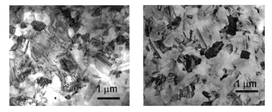
Figure 2.13 shows two pieces of polycrystalline Si with two different
doping concentrations. However, the grain size shows in both subfigures nearly
the same size distribution from a macroscopic point of view.
From a microscopic point of view, for instance in a window
![]() microns, the area would include either 1 or a few grains.
If the resistivity would be considered of this fictive area, the difference
would be a factor 2 or even more.
microns, the area would include either 1 or a few grains.
If the resistivity would be considered of this fictive area, the difference
would be a factor 2 or even more.
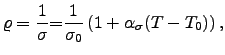
To describe materials from a macroscopic point of view, there are two main approaches. The first approach describes the conductivity or the resistivity of the materials, which requires the knowledge of the microstructure. If the material cannot be assumed to be an isotropic bulk material, the observed behavior has to be described with anisotropic material models. However, the microstructure is often not well known. Therefore, characteristic material layers were measured to provide characteristic material parameters such as the temperature coefficients for the conductivities or the sheet resistance, which is mainly determined by the fabrication process. This provides an important advantage for the design in terms of computational effort for the evaluations of the models.
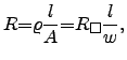
The sheet resistance ![]() is defined as resistance for a specific layer
thickness
is defined as resistance for a specific layer
thickness
![]() as
as
| (2.135) |
 |
(2.136) |
A common method to account for difficult thermal effects for instance during self-heating is to apply a correction term to the well known parameters, which change with temperature, power density, or electric field. If for instance the temperature dependence is modeled, a polynomial approach is often used
Such polynomial models are found in literature for nearly every material which
shows rather smooth behavior without any abrupt property transitions.
However, if the impact of a particular observable
is too drastic, a different model has to be developed and to be applied to
describe the observed behavior more accurately.