Next: 3. Thermal Models Up: 2.4 Material Deposition Previous: 2.4.2 Deposition of SiO Contents
Another important process technology is the electro plating for the Cu interconnect metal structures. In this technology, the structure is patterned by etching the shape of the structure in the underlying inter-layer dielectric (ILD) materials. After the patterning, a very thin barrier layer is deposited on top of the etched structure [32,158,159,160] (e.g. Ta/TaN, TiN, CoWP, NiMoP, NiMoB). On top of that layer a seed layer is deposited which supports better adhesion of the Cu on the underlying material and acts as catalytic material during the plating process as well. Typical materials for these seed layers are compounds which include the material Pd or other compounds of polymers and organic materials.
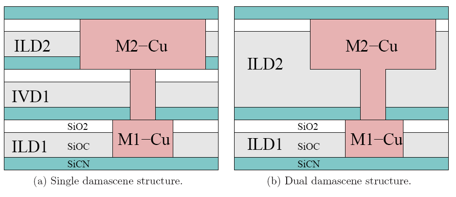 |
The original deposition process (damascene process) was designed to process each
layer on its own. Hence, the vias and the metalization levels had different
process steps and demand a sequence of cleaning, material deposition, CMP,
and another cleaning step for each layer.
A Cu technology using this sequence for its metalization levels as well as
for its inter layer dielectrics (ILDs) and inter via dielectrics (IVDs) is
called single damascene process.
A simplified cut through a single damascene processed wafer is depicted
in Figure 2.16a, where a typical structure, showing a
level-oriented material compositions, is presented.
Here, each level requires its own cap layer or etch stop layer, a separate
ILD layer, and at the top there is a need for a material -- for instance
![]() -- that can be polished together with the interconnect metal copper.
-- that can be polished together with the interconnect metal copper.
Alternatively, a dual damascene technology combines certain similar process steps to one reducing the number of process steps and thus the time and costs required to build the back end of line (BEOL) stack. Hence the dual damascene process fabricates the IVD and the metalization layer at once. Obviously, as can be seen in Figure 2.16b, the metalization level has an increased thickness because the interconnect lines as well as the vias are included in a single metalization level.