Next: 3.7.2 Mean Time To Up: 3.7 Interconnect Reliability Previous: 3.7 Interconnect Reliability Contents
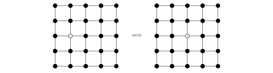
Current transport involves two types of charge carriers: electrons and holes (defect electrons), and ions and vacancies (defect ions) as depicted in Figure 3.2. While the first charge carrier type is normally used for the device operation, the second produces disadvantageous effects and causes tremendous failure. For instance, if ions are transported through the interconnect lines the resulting ion current has also to be considered as mass flux.
Atoms on ideal crystal lattices need a high activation energy to change the position on the lattice (cf. Figure 3.2). Unregularities in the crystal significantly descrease the activation energy. Such promoting factors are interstitials and the grain structure due to irregular crystal growth, and impurities in the grain as well as at grain boundaries at the material interfaces (cf. Figure 3.3). These factors are advanced by additional energy provided by elevated temperatures in the structures due to self-heating and external heat sources, where the increasing current densities reach critical values at which self-heating effects dominate the reliability issues.
At elevated temperatures, the ions and defects have an increased diffusivity, which is further enhanced by external applied current densities. The atoms move in the direction given by the electrons. At a certain point in time, a microscopic hole (void) is seeded on the one side and a pocket (hillock) is formed on another side. The void can cause an opening of an interconnect line while the hillock might shorten two adjacent interconnect structures. Both scenaria yield fatal errors.
The dynamics of moving atoms and their vacancies can be described by a drift-diffusion model similar to that for electrons in semiconductor materials in (2.14) and (2.15), but with different mobilities and diffusion coefficients. A model for the mobility of vacancies
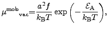 |
(3.30) |
| (3.31) |
 |
Regions in which the mechanical stress is notably important are areas where high current densities occur simultaneously with high temperature gradients [100]. In these regions with very high current densities and elevated temperatures, electro-migration can be observed [208]. The occurrence of this failure type is accelerated with increasing temperature. This effect can be used to estimate reliability and life time. However, this accelerated test method is only an estimation for the worst case.
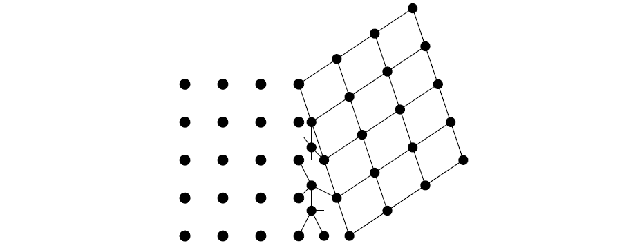
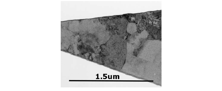
The previously presented models have assumed that the shape, the orientation, and the distribution of the size of the grains does not affect the stress distribution. Unfortunately, the grain boundaries are layers of a finite thicknesses and the mechanical constants vary along these structures. Due to the different crystal orientations in adjacent grains, the same material in different grains behaves slightly different even if the same mechanical load is applied [209]. For instance, the diffusion along paths through the interconnect results in different current densities according to the corresponding local crystal structure. Apparently, the diffusion coefficients depend also on an activation energy [163,33], which itself is a function of the material adhesion and the regularity of the lattice, as shown for Cu in Figure 3.4. A cross section of a Cu interconnect structure is shown in Figure 3.5, where no information about the distribution of the grain sizes is given.
 |
The uncertainty of the position and the size of grain boundaries are new
critical parameters for reliability investigations. Unfortunately, these
parameters cannot be determined excactly in advance. However, a statistical
description of these parameters can be applied and provides rather good
agreement with measurements but does not account for the degradation effects in
the metal, the moving grain boundaries, the movements of the defect location, or
recrystallization [164].
As Tab. 3.5 shows, copper ions at lattice sites in bulk-sized grains have the tendency to diffuse not as much as near the surface. For ions located near the interfaces (grain boundaries or material interfaces) the diffusion constant nearly doubles. For copper atoms at surfaces the activation energy is only one third of that in the bulk material. Hence, material regions near surfaces and material interfaces have to include the ion diffusion of copper rigorously to predict their reliability properly.
The material
![]() has been substituted by
has been substituted by
![]() to increase the intrinsic activation
energy for electro-migrationfrom 0.6 eV for bulk
to increase the intrinsic activation
energy for electro-migrationfrom 0.6 eV for bulk
![]() to
to
![]() for bulk
for bulk
![]() [207].
Cu has a higher melting temperature. Incidentally, this substitution should have
caused less problems with electro-migration.
However, the material interface conditions were not considered in the very
beginning of the transition.
In the common Cu technology, the barrier and cap layers for interconnect lines
increase the mechanical weakness of the interfaces to Cu, which cause an
additional reduction of the activation energy.
[207].
Cu has a higher melting temperature. Incidentally, this substitution should have
caused less problems with electro-migration.
However, the material interface conditions were not considered in the very
beginning of the transition.
In the common Cu technology, the barrier and cap layers for interconnect lines
increase the mechanical weakness of the interfaces to Cu, which cause an
additional reduction of the activation energy.
Another contribution to reliability reduction can be found in the unfavorable
microstructure of the materials used in interconnects.
The microstructure of
![]() is formed during electro-plating, where the final shape of
the grains is determined by exogenous parameters.
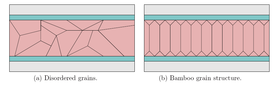
The microstructures of two different electro-plating fabrication process are
depicted in Figure 3.6a and Figure 3.6b, where in Figure 3.6a
a technology is presented where the microstructure of Cu cannot be controlled. A
better result can be achieved if the process temperature, and the seed and
barrier layers can be appropriately controlled.
As a result, the grains evolve homogeneously with similar shape and with nearly
the same size distribution, as shown in Figure 3.6,
where Figure 3.6b shows a 'bamboo' structure, which has the benefit
that the current through such structured interconnects flows perpendicular to
most parts of the grain boundaries.
is formed during electro-plating, where the final shape of
the grains is determined by exogenous parameters.
The microstructures of two different electro-plating fabrication process are
depicted in Figure 3.6a and Figure 3.6b, where in Figure 3.6a
a technology is presented where the microstructure of Cu cannot be controlled. A
better result can be achieved if the process temperature, and the seed and
barrier layers can be appropriately controlled.
As a result, the grains evolve homogeneously with similar shape and with nearly
the same size distribution, as shown in Figure 3.6,
where Figure 3.6b shows a 'bamboo' structure, which has the benefit
that the current through such structured interconnects flows perpendicular to
most parts of the grain boundaries.
The most significant contribution to electro-migration is due to surface
diffusion, which is also a main factor for reliability issues in
![]() interconnect lines.
The bamboo structure in Figure 3.6b could easily be enhanced further
by chemical-mechanical polishing (CMP), where the upper zones of the bamboo
structures can be removed. Hence, the removed upper side is a step towards an
ideal microstructure by minimizing the number of grain boundaries not
perpendicular to the average current density vector.
Removing the most upper region of
interconnect lines.
The bamboo structure in Figure 3.6b could easily be enhanced further
by chemical-mechanical polishing (CMP), where the upper zones of the bamboo
structures can be removed. Hence, the removed upper side is a step towards an
ideal microstructure by minimizing the number of grain boundaries not
perpendicular to the average current density vector.
Removing the most upper region of
![]() , the original
, the original
![]() structure has to be
deposited with a higher thickness as required. The additional
structure has to be
deposited with a higher thickness as required. The additional
![]() is removed
by a CMP process.
With that procedure, the upper critical zone is removed from the copper
surface. The bottom of the
is removed
by a CMP process.
With that procedure, the upper critical zone is removed from the copper
surface. The bottom of the
![]() surface as well as the side walls are treated
by special seed and barrier layers, which prevent at one hand the diffusion
of
surface as well as the side walls are treated
by special seed and barrier layers, which prevent at one hand the diffusion
of
![]() into the dielectrics. On the other hand these layers act as
catalysts during the initial
into the dielectrics. On the other hand these layers act as
catalysts during the initial
![]() deposition to form an ``ideal'' initial
microstructure.
deposition to form an ``ideal'' initial
microstructure.
During operation, elevated temperature and high current densities, it can happen
that the vacancy concentration due to electro-migration inside a critical
material region exceeds a certain limit
(vacancy concentration ![]() number of atoms per unit cell of the basis
interconnect material).
In that case, a void has been seeded in that
region [213]. This behavior is called inverse clustering because
the modeling approach considers the accumulation of precipitates at the
beginning in terms of a vacancy concentration in the microscopic level and at the
intermediate state via voids as a macroscopic description.
With a seeded void, an additional surface has been introduced into the
material region which has been previously assumed to be bulk-like.
This surface results in a region with reduced activation energy and therefore
promotes the diffusion of
number of atoms per unit cell of the basis
interconnect material).
In that case, a void has been seeded in that
region [213]. This behavior is called inverse clustering because
the modeling approach considers the accumulation of precipitates at the
beginning in terms of a vacancy concentration in the microscopic level and at the
intermediate state via voids as a macroscopic description.
With a seeded void, an additional surface has been introduced into the
material region which has been previously assumed to be bulk-like.
This surface results in a region with reduced activation energy and therefore
promotes the diffusion of
![]() atoms, thus accelerating the growth of the void.
A growing void yields a material transport from the void site to a physical
barrier material where a pocket (hillock) is built.
The voids itself may cause an interruption of the interconnect line, while the
materials pocket may cause a shortening between two adjacent interconnect
structures.
Providing a reservoir of the migrating materials is an
improvement [214], but only of limited help for the interconnect
reliability. While the time that is needed to seed and form a void is
considerably high, the time needed to move the voids and form hillocks and big
voided regions is orders of magnitude less than the time for the seeding and
forming process.
atoms, thus accelerating the growth of the void.
A growing void yields a material transport from the void site to a physical
barrier material where a pocket (hillock) is built.
The voids itself may cause an interruption of the interconnect line, while the
materials pocket may cause a shortening between two adjacent interconnect
structures.
Providing a reservoir of the migrating materials is an
improvement [214], but only of limited help for the interconnect
reliability. While the time that is needed to seed and form a void is
considerably high, the time needed to move the voids and form hillocks and big
voided regions is orders of magnitude less than the time for the seeding and
forming process.
Better results for the improvement of reliability can be obtained if the roots of the problem are rigorously tackled. Those are the high current densities, the reduced line dimensions, the resulting elevated temperatures, and the weak material interfaces with their poor adhesion on certain materials causing a considerable problem in addition to the natural material diffusion, the current density, and the high temperatures. The main reason for enhanced surface diffusion and electro-migration has been identified as the unfavorable crystal structure close to the material interfaces. If one can provide an (ideal) crystallized Cu layer up to the material interface, the Cu atoms would be located at more or less ideal lattice sites and thus would require a higher activation energy to move.
 |
The introduction of new interface materials such as
![]() and
and
![]() have provided
promising results by slightly rising the activation energy and lowering the
migration tendency.
However, the fundamental problem of not ideal crystal structures with high
diffusion constants has not been tackled. Only with the introduction of new
porous barrier materials, the electro-migration effects has been significantly
reduced.
If the pores of these materials exceed a certain size,
have provided
promising results by slightly rising the activation energy and lowering the
migration tendency.
However, the fundamental problem of not ideal crystal structures with high
diffusion constants has not been tackled. Only with the introduction of new
porous barrier materials, the electro-migration effects has been significantly
reduced.
If the pores of these materials exceed a certain size,
![]() atoms have the possibility to move into those pores. This yields a starting
crystallization very close to the surface, actually in the
barrier layer (cf. Figure 3.7).
That provides a good alternative to
atoms have the possibility to move into those pores. This yields a starting
crystallization very close to the surface, actually in the
barrier layer (cf. Figure 3.7).
That provides a good alternative to
![]() and
and
![]() coatings.
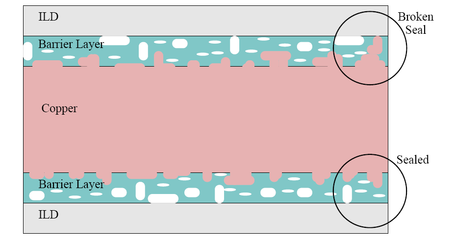
The deposition of such porous materials requires a guaranteed seal
barrier coating. With completely sealed coatings, the
coatings.
The deposition of such porous materials requires a guaranteed seal
barrier coating. With completely sealed coatings, the
![]() atoms diffuse into the
ILDs, causing serious problems as already discussed.
atoms diffuse into the
ILDs, causing serious problems as already discussed.
Unfortunately, the COO of these porous materials is considerably large. Thus, the
implementation of such materials might take some time in the common
Cu technology nodes.
With the increasing number of
high-![]() and
low-
and
low-![]() materials, where most
of them are porous materials, also the porous barrier layers will be
available in the near future.
materials, where most
of them are porous materials, also the porous barrier layers will be
available in the near future.